Overview
This application note describes how to implement a circuit to trigger an automatic power-on event at power up of the AM57x. This solution is appropriate for any custom applications that cannot support a manual power button.
Recommended Circuit Implementation
The schematic of the recommended circuit solution is shown in Figure 1. The design has been simulated via LTspice, as well as physically built and tested. The measured X_PWRON response of the physical implementation is shown in Figure 2. Further information and results are detailed in the following sections of this Application Note.


Figure 2: X_PWRON Response of Recommended Circuit Design
The table below lists the recommended components to use in the implementation of this design. The reference designators used are based on the schematic shown in Figure 1.
| Reference Designator | Recommended Part Number | Description |
|---|---|---|
| R1 | - | 10kΩ |
| R2 | - | 10kΩ |
| R3 | - | 143kΩ |
| C1 | - | 1uF |
| C2 | - | 100nF |
| C3 | - | 100nF |
| D1 | LL42-GS08 | Small Signal Schottky Diode (Vishay Semiconductors) |
| D2 | LL42-GS08 | Small Signal Schottky Diode (Vishay Semiconductors) |
| A1 | SN74LVC1G17DCK | Single Schmitt-Trigger Buffer (Texas Instruments) |
| M1 | 2N7002 | N-Channel MOSFET (NXP Technologies) |
Although these particular parts are recommended, they can be replaced as necessary based on limitations of cost, space, etc... When replacing these components, take care in the selection of the passive values as the response timing may change. The X_PWRON delay can be adjusted as described in the following sections of this application note. A package size of 0805 is recommended for the passive components for easier hand rework when replacing these parts.
Actual values of these passive components may require tuning for specific use cases.
Note that earlier versions of the AM57x SOM (PCM-057.A5 and earlier) populate C251 with a 1uF capacitor, which is connected between X_PWRON and ground. This capacitor will introduce further delay on the X_PWRON rise/fall time, potentially causing the board not to respond or boot as expected. The design was updated to populate C251 with a smaller 0.1uF capacitor, which results in an X_PWRON response similar to Figure 2. Consider this capacitor value when implementing this design with an older version of the SOM.
Troubleshooting
Please refer to the following timing diagram. Each window of time labeled 1, 2, 3, etc... will be referred to as T1, T2, T3, etc... respectively.

Issue #1 - Booting is inconsistent, unreliable, or not working at all.
Solution #1 - This may be a result of X_PWRON being toggled low too soon before VCC_3V3 is on and stable. For reliable booting, ensure that T3 is at least ~5.5ms to allow the device to arrive at the 'OFF' state from the 'NO SUPPLY' state (further details available in this application note). Increase the R3 and C2 values to increase the delay time before X_PWRON is toggled low.
Issue #2 - Board begins to boot, but then shuts off after a few seconds.
Solution #2 - This may be a result of X_PWRON being toggled low for too long, triggering a 'long press' at the PMIC (typically a few seconds). When a long press is detected the PMIC will transition the system to the OFF state. The X_PWRON low time, T4, can be adjusted by decreasing the values of R2 and C3.
Circuit Design
This circuit will be powered by the main 3.3V rail (labeled VCC_3V3_IN on the AM57x SOM). The circuit consists of an RC delay stage, a Schmitt trigger stage, and an RC + FET circuit to generate the X_PWRON pulse.
The RC delay provides control over the X_PWRON delay. R3 and C2 can be tuned to ensure that the VCC_3V3 rail is powered and stable long enough before toggling X_PWRON. The D1 diode is included to discharge C2 quickly after VCC_3V3 is powered off. This ensures that C2 will be discharged even in the event of a quick power cycle, keeping the RC delay consistent between power cycles. Without this diode C2 may only discharge slightly before power is reapplied, which could cause a shorter delay (or even no delay at all).
The Schmitt trigger stage is intended to prevent noise on the VCC_3V3 rail from triggering the X_PWRON transition. If the input to the Schmitt trigger is 'bouncing' around or noisy, it will filter this out and only transition X_PWRON when a significant change in the input occurs.
The third stage is implemented to generate the X_PWRON pulse low at the rising edge of the Schmitt trigger output. By gating the M1 NMOS with this RC combination, the X_PWRON will toggle low then high only once (rather than remaining low after toggling). D2 is used to clamp the negative voltage caused by the falling edge of the Schmitt trigger output. During quick power cycles this could prevent the C1 capacitor from charging up to a level that will properly bias the M1 FET. Therefore D2 is recommended for consistent behaviour during quick power cycles. An additional RC delay is added before the gate of the NMOS to slow down the switching time of the FET. This timing can be adjusted to prevent overshoot and other undesired behavior caused by the fast transitions at the gate of the FET.
LTspice Simulation
Figure 3 below shows how the circuit was simulated in LTspice. The 3.3V supply was driven by a pulse source to simulate a quick power cycle. A number of waveforms were captured to test the general behavior and response of the design and to verify its stability. The processor and PMIC datasheets do not seem to provide a specific amount of time that the 3.3V rail should be powered up before toggling X_PWRON. However, these timings can be adjusted by the passive components as described in the Schematic Design section if issues arise during testing and validation.
The rise time was simulated as 4ms based on the AM57x carrier board 3.3V switching regulator design. A load of 100uF and 3.3 ohms was also added to simulate the load on the 3.3V rail. All of these values may change based on the target design/load, so the passive component values may need to be adjusted to optimize the circuit response.

Figure 3: Simulation Circuit Example
R4 is included to represent the 10k pull-up resistor on the AM57x SOM, which is actually labeled as R158. If R158 is populated, an additional pull-up resistor should NOT be added.

Figure 4: VCC_3V3 vs. X_PWRON
Figure 5 and 6 show the response of the RC delay with and without the D1 diode. Implementing D1 allows the C2 capacitor to discharge faster when 3V3 is powered off. When power is re-applied quickly, the RC delay circuit will then maintain a delay much closer to its expected delay value as C2 will not be starting partially charged. Note that even with D1 it is possible that C2 does not completely discharge when 3.3V power is applied immediately (though discharging is still improved).

Figure 5: RC Delay Quick Power Cycle without D1

Figure 6: RC Delay Quick Power Cycle with D1
Figure 7 and 8 show the response of the FET gate input with and without the D2 diode. The R1 and C1 circuit is intended to trigger on the rising edge of the 3.3V rail, however on the falling edge it will drive a negative voltage at its output. This undesired response can be reduced by clamping the output with D2. Without D2 (during a fast power cycle) the negative voltage will cause the signal to rise to its positive level much slower as the C1 charge reverses. If the power cycle is fast enough this can prevent the M1 FET from being properly biased, and therefore not trigger X_PWRON as expected.

Figure 7: R1/C1 Output without D2

Figure 8: R1/C1 Output with D2
Figure 9 and 10 show the response of X_PWRON with and without an additional RC delay at the FET's gate input. Without this RC delay it seems the switching of the M1 NMOS is too fast, which is causing spikes on X_PWRON during the edge transitions of the gate input. By adding a small RC delay, the switching time can be slowed down so that X_PWRON does not experience these signal spikes.

Figure 9: R1/C1 Output without RC delay

Figure 10: R1/C1 Output with RC delay
Figure 11 shows the response of X_PWRON when the power is cycled during the low pulse of X_PWRON.The circuit behaves properly except for a small spike after the first falling edge of X_PWRON. This is likely due to the 3.3V rail being powered off quickly, which causes the FET to 'switch off' sooner. This then causes X_PWRON to follow VCC_3V3 (via the pull-up), which is still discharging towards 0V. This should not be an issue, but if this behavior is not desired the R2/C3 delay can be adjusted so that the transition at the M1 gate is slower. For example, Figure 12 shows the response when R2 is replaced with a 30k ohm resistor (this X_PWRON spike is no longer present).
Increasing the R2/C3 delay will increase the rise and fall times of the M1 gate waveform. Therefore it will take longer to reach the proper M1 biasing voltage, which will reduce the time X_PWRON is pulsed low. If this rise time is too long, then the gating signal will begin to fall to 0V again before switching the M1 FET on. This will prevent X_PWRON from toggling low at all. Take care in selecting the values of the passive components and the M1 NMOS.

Figure 11: VCC_3V3 Power Cut Behavior During X_PWRON Low Pulse

Figure 12: VCC_3V3 Power Cut Behavior During X_PWRON Low Pulse with R2 = 30k
Physical Circuit Testing
This circuit was implemented on a PHYTEC GPIO Expansion Board to test the actual behavior of the design.
The following two figures show the response of X_PWRON at power up. This output is NOT yet connected to the X_PWRON signal on the AM5 kit to first verify the design functionality.

Figure 13: X_PWRON Response Isolated from AM5

Figure 14: X_PWRON Response Isolated from AM5 Zoomed
After verifying the circuit produces the correct X_PWRON response, this output was connected to the X_PWRON signal on the AM5 kit. With the circuit driving X_PWRON and the current timings, the board does not boot consistently. It seems the time between VCC_3V3 stabilizing and X_PWRON toggling low is not long enough. This was adjusted by replacing R3 with a 55k resistor (rather than a 10k), and resulted in consistent booting. The new timing is shown in the following figures.

Figure 15: X_PWRON Low Delay with R3=55k

Figure 16: X_PWRON Toggle Delay after VCC_3V3
These passive values may need to be adjusted further to optimize the timing and behavior.

Figure 17: FET Gate Input Response to Quick Poweroff
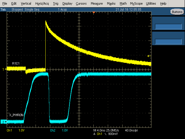
Figure 18: X_PWRON vs R1/C1 Response
A quick power cycle was implemented to analyze the behavior of the circuit under this condition. As shown in Figure 18, the response of the R1/C1 stage has a small positive spike before its typical rise response. To debug the root cause of this, the Schmitt trigger stage was further analyzed during a quick power cycle. Figure 20 shows the Schmitt trigger response at initial power up after the board has remained off for some time. However, when power is then quickly cycled after being powered up, the Schmitt trigger output has a small, positive spike as shown in Figure 21. This is likely due to the slower fall time of the VCC_3V3 rail at power off. Looking into the SN74LVC1G17 Schmiit Trigger datasheet it was found that the minimum recommended operating voltage is 1.65V. As shown in Figure 20, once VCC_3V3 approximately reaches this 1.65V, the Schmitt output is driven low and then responds as expected. Since the VCC_3V3 rail has not fallen to 0V at this point, there is some voltage remaining at the Schmitt input. It seems that with a non-zero voltage at the input while operating under 1.65V, the Schmitt trigger is in an undefined state and could have a much smaller or unpredictable positive-going input threshold voltage.

Figure 19: X_PWRON vs R1/C1 Response During Quick Power Cycle

Figure 20: Schmitt Trigger Response to Initial Power Up

Figure 21: Schmitt Trigger Response to Quick Power Cycle
The quick power cycle case does not seem to impact the intended response of the circuit however. As shown in Figure 22, the R2/C3 delay prevents this spike from rising to a level to bias the FET and drive X_PWRON low too early. So these passive values could be adjusted if necessary. However, if this is undesired, it may be resolved by implementing a method for draining VCC_3V3 faster.

Figure 22 : FET Input Response to Quick Power Cycle Spike
After further research through the PMIC datasheet, the following information was found regarding the definition of the 'OFF' state:
" The device is powered by a valid supply on the system power rail (VCC1 > VSYS_LO) and it is waiting for a start-up event or condition. All device resources are in the OFF state. The approximate time for device to arrive to the OFF state from the NO SUPPLY state, without considering the rise time of VSYS and the settling time of the VSYS_LO comparator, is approximately 5.5ms."
X_PWRON should at least be delayed long enough for the device to arrive in the OFF state, so a power-up event is recognized properly. With R3 = 55k, the current delay is measured around ~4 ms using real components. It is recommended that R3 be increased even further to provide a safer delay margin. Replacing R3 with a 143k resistor, the delay was measured as ~10 ms. It is recommended to use a 143k resistor for R3.