...
This hardware manual describes the PCL-069 System on Module, referred to as phyCORE®-i.MX 8M Mini, and the PBA-C-15, referred to as phyBOARD®-Polis. This manual also specifies the phyCORE-i.MX 8M Mini and phyBOARD-Polis' design and function. Precise specifications for the NXP® Semiconductor i.MX 8M Mini microcontrollers can be found in the i.MX 8M Mini Microcontroller Data Sheet/Reference Manual.
| Scroll Indexterm | ||||
|---|---|---|---|---|
|
Design Considerations
The schematics shown in this hardware manual are believed to be correct. However, correctness can not be guaranteed. The schematics have been pulled from PHYTEC's designs that have been built, tested, and is known to work. The schematics have been re-formatted to fit better in this hardware manual.
...
http://www.phytec.de/de/leistungen/entwicklungsunterstuetzung.html
or
http://www.phytec.eu/europe/oem-integration/evaluation-start-up.html
...
Ordering Information
The part numbering of the phyCORE has the following structure:
...
...
Product Specific Information and Technical Support
In order to receive product-specific information on all future changes and updates, we recommend registering at:
http://www.phytec.de/de/support/registrierung.html or http://www.phytec.eu/europe/support/registration.html
...
| Note | ||
|---|---|---|
| ||
Assembly Options include a choice of Controller, RAM (Size/Type), Size of NAND Flash, interfaces available, vanishing, temperature range, as well as other features. Please contact our sales team to get more information on the ordering options available. |
...
Declaration of Electro Magnetic Conformity of the PHYTEC phyCORE®‑i.MX 8M Mini
...
PHYTEC System on Module (henceforth products) are designed for installation in electrical appliances or as dedicated Evaluation Boards (i.e.: for use as a test and prototype platform for hardware/software development) in laboratory environments.
| Warning | ||
|---|---|---|
| ||
PHYTEC products lacking protective enclosures are subject to damage by ESD and, therefore, must be unpacked, handled, or operated in environments in which sufficient precautionary measures have been taken in with respect to ESD - dangers. Only appropriately trained personnel such as qualified electricians, technicians, and engineers should handle and/or operate these products. Moreover, PHYTEC products should not be operated without protection circuitry if connections to the product's pin header rows are longer than 3 m. |
PHYTEC products fulfill the norms of the European Union’s Directive for Electro Magnetic Conformity in accordance with the descriptions and rules of usage indicated in this hardware manual (particularly in with respect to the pin header row connectors, power connector, and serial interface to a host-PC).
| Tip | ||
|---|---|---|
| ||
Implementation of PHYTEC products into target devices, as well as user modifications and extensions of PHYTEC products, is subject to renewed establishment of conformity to and certification of Electro Magnetic Directives. Users should ensure conformance following any modifications to the products as well as the implementation of the products into target systems. |
...
Product Change Management and Information Regarding Parts Populated on the SOM / SBC
...
| Anchor | ||||
|---|---|---|---|---|
|
With the purchase of a PHYTEC SOM / SBC you will, in addition to our hardware and software possibilities, receive free obsolescence maintenance service for the hardware we provide. Our PCM (Product Change Management) team of developers is continuously processing all incoming PCN's (Product Change Notifications) from vendors and distributors concerning parts that are used in our products. Possible impacts on the functionality of our products due to changes in functionality or obsolesce of certain parts are constantly being evaluated in order to take the right measures either in purchasing decisions or within our hardware/software design.
...
- Ensure long-term availability by stocking parts through last-time buy management according to product forecasts.
- Offer long-term frame contracts to customers.
...
- Avoid impacts on product functionality by choosing equivalent replacement parts.
- Avoid impacts on product functionality by compensating for changes through hardware redesign or backward-compatible software maintenance.
- Provide early change notifications concerning functional, relevant changes to our products.
We refrain from providing detailed part-specific information within this manual, which can be subject to continuous changes, due to part maintenance for our products.
In order to receive reliable, up-to-date, and detailed information concerning parts used for our product, please contact our support team through the contact information given within this manual.
...
PHYTEC Documentation
...
PHYTEC will provide a variety of hardware and software documentation for all of our products. This includes any or all of the following:
...
| Tip | ||
|---|---|---|
| ||
The BSP delivered with the phyCORE-i.MX 8M Mini includes drivers and/or software for controlling all components such as interfaces, memory, etc. Programming close to hardware at register level is not necessary in most cases. For this reason, this manual contains no detailed description of the controller's registers or information relevant to software development. Please refer to the NXP i.MX 8M Mini Reference Manual, if such information is needed to connect customer-designed applications. |
...
Conventions
...
The conventions used in this manual are as follows:
- Signals that are preceded by an "n", "/", or “#”character “#” character (e.g.: nRD, /RD, or #RD), or that have a dash on top of the signal name (e.g.: RD) are designated as active low signals. That is, their active state is when they are driven low, or are driving low.
- A "0" indicates a logic zero or low-level signal, while a "1" represents a logic one or high-level signal.
- The hex - numbers given for addresses of I2C devices always represent the 7 MSB of the address byte. The correct value of the LSB which depends on the desired command (read (1), or write (0)) must be added to get the complete address byte. E.g. given address in this manual 0x41 => complete address byte = 0x83 to read from the device and 0x82 to write to the device
- Tables that describe jumper settings show the default position in bold, blue text.
...
Types of Signals
Different types of signals are brought out at the phyCORE-Connector. The following table lists the abbreviations used to specify the type of signal.
| Scroll Title | ||||||||||||||||||||||||||||||||||||||||||||||||||||||||||||||||||||||||||||||||||||||||||||
|---|---|---|---|---|---|---|---|---|---|---|---|---|---|---|---|---|---|---|---|---|---|---|---|---|---|---|---|---|---|---|---|---|---|---|---|---|---|---|---|---|---|---|---|---|---|---|---|---|---|---|---|---|---|---|---|---|---|---|---|---|---|---|---|---|---|---|---|---|---|---|---|---|---|---|---|---|---|---|---|---|---|---|---|---|---|---|---|---|---|---|---|---|
| ||||||||||||||||||||||||||||||||||||||||||||||||||||||||||||||||||||||||||||||||||||||||||||
|
...
Abbreviations and Acronyms
| Anchor | ||||
|---|---|---|---|---|
|
Many acronyms and abbreviations are used throughout this manual. Use the table below to navigate any unfamiliar terms used in this document.
...
Independent research indicates approximately 70 % of all EMI (Electro-Magnetic Interference) problems are caused by insufficient supply voltage grounding of electronic components in high-frequency environments. The phyCORE board design features an increased pin package, which allows for the dedication of approximately 37 % of all connector pinson the phyCORE boards to Ground. This improves EMI and EMC characteristics and makes it easier to design complex applications meeting EMI and EMC guidelines using phyCORE boards, even in high-noise environments.
phyCORE boards achieve their small size through modern SMT and multi-layer design. Due to the complexity of our modules, 0201-packaged SMT components and laser-drilled microvias are used on the boards, providing phyCORE users with access to this cutting-edge miniaturization technology for integration into their own design.
The phyCORE‑i.MX 8M Mini is a sub-miniature (37 mm x 40 mm) soldered System on Module populated with the NXP® Semiconductor i.MX 8M Mini microcontroller. Its universal design enables its insertion in a wide range of embedded applications. All controller signals and ports extend from the controller to a 1,27mm pitch BGA Ball. Each signal ball has an associated GND pin which ensures the GND reference for each signal. The ball packages are placed in lines. There is enough space between lines to ensure the possibility of easy routing out of the package. Signal balls for a high-speed signal like HDMI are placed on the outer lines, making it easy to route to the top layer of the carrier board. The SOM is designed to support carrier boards with as little few as 6 layers to reduce PCB costs. For proper EMC characteristics, it is necessary to place the processor caps directly under the SOM. This required a hole in the carrier board.
The descriptions in this manual are based on the NXP® Semiconductor i.MX 8M Mini. Descriptions of compatible microcontroller derivative functions are not included, as such functions are not relevant for the basic functioning of the phyCORE‑i.MX 8M Mini.
...
...
phyCORE‑i.MX 8M Mini Features
...
...
The phyCORE‑i.MX 8M Mini offers the following features:
- Insert-ready, sub-miniature (37 mm x 40 mm) System on Module (SOM) sub-assembly in low EMI design, achieved through advanced SMD technology
- Mounted using BGA Technology
- Populated with the NXP® Semiconductor i.MX 8M Mini microcontroller (BGA486 packaging)
- 1.6 GHz core clock frequency (up to 1.8 GHz)
- Boot from different memory devices (eMMC standard)
- Single supply voltage of +3.3 V with onboard power management
- All controller-required supplies are generated onboard
- Improved interference safety achieved through multi-layer PCB technology and dedicated ground pins
2 GB (up to 4 GB)
Single cite citeID 1 The maximum memory size listed as of the printing of this manual.
Please contact PHYTEC for more information about additional or new module configurations available.) LPDDR4 RAM
- 4 GB (up to 32 GB
) onboard eMMCSingle cite short citeID 1 - 4 kB
I2C EEPROMSingle cite short citeID 1 - 2x High-Speed USB 2.0 OTG interfaces
1x 10/100/1000 MBit Ethernet interface (if Ethernet transceiver is mounted)
Single cite citeID 2 Please refer to the order options described in the L-862e.Ax phyCORE-i.MX 8M Mini/phyBOARD-Polis (1518.1a / 1532.1) HW Manual Head
or contact PHYTEC for more information about additional module configurations.- One RGMII interface at TTL level (if Ethernet transceiver is not mounted)
Single cite short citeID 2 - Three I2C interfaces
- Two SPI interfaces
- One PCIe interface
- Four UART interfaces
- Four PWM outputs
- One LVDS interface (if MIPI-DSI to LVDS converter is mounted)
Single cite short citeID 2 - One MIPI DSI interface (if MIPI-DSI to LVDS converter is not mounted)
Single cite short citeID 2 - One MIPI CSI camera interface
- One 4-Bit SD-Card interface
- One 8-Bit SDIO interface
- SAI audio interface
- Internal RTC
- Available for different temperature grades (L-862e.Ax phyCORE-i.MX 8M Mini/phyBOARD-Polis (1518.1a / 1532.1) HW Manual Head)
| Cite summary | ||||
|---|---|---|---|---|
|
...
...
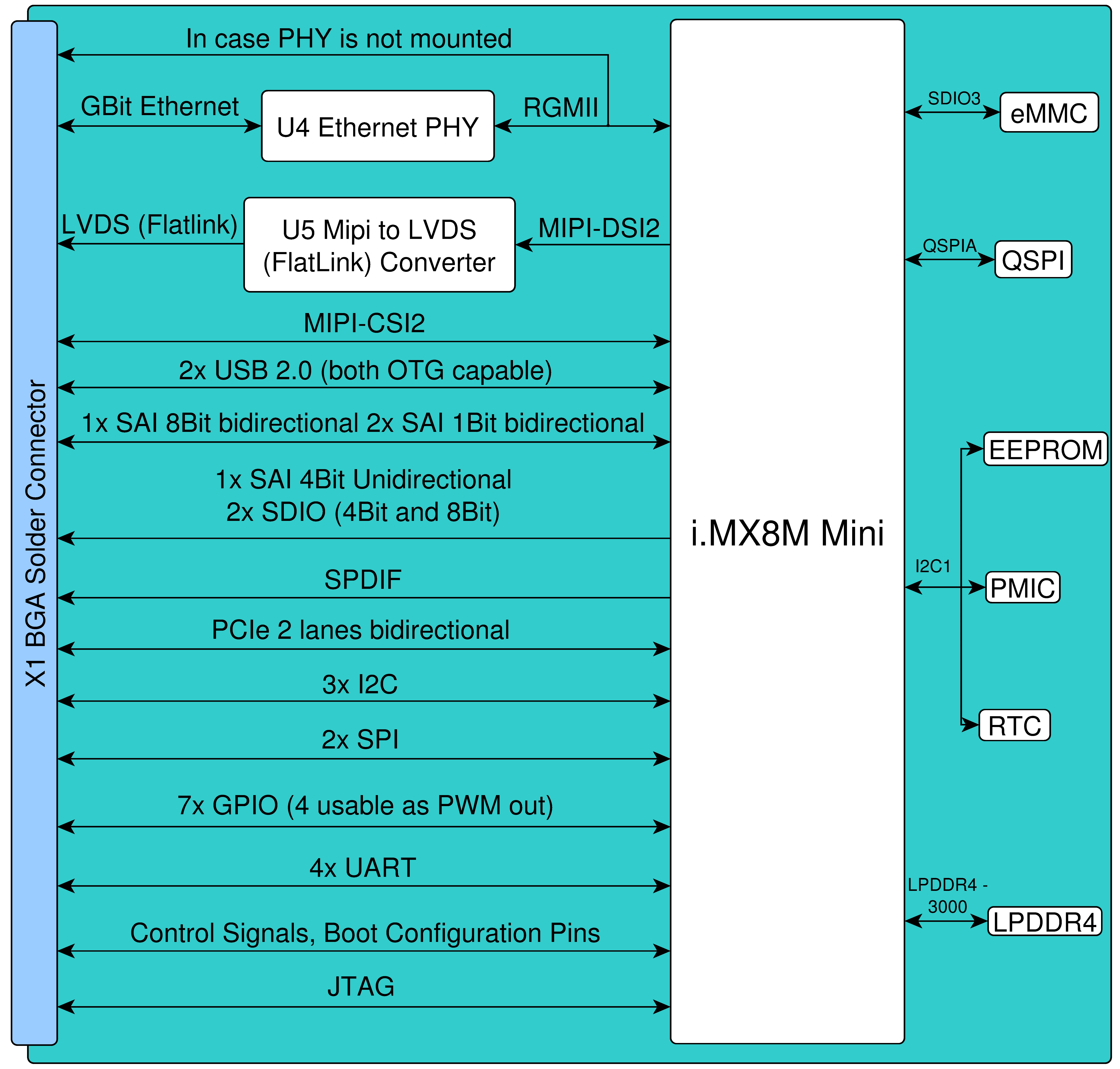
phyCORE-i.MX 8M Mini Block Diagram
...
| Anchor | ||||
|---|---|---|---|---|
|
| Scroll Title | ||||
|---|---|---|---|---|
| ||||
...
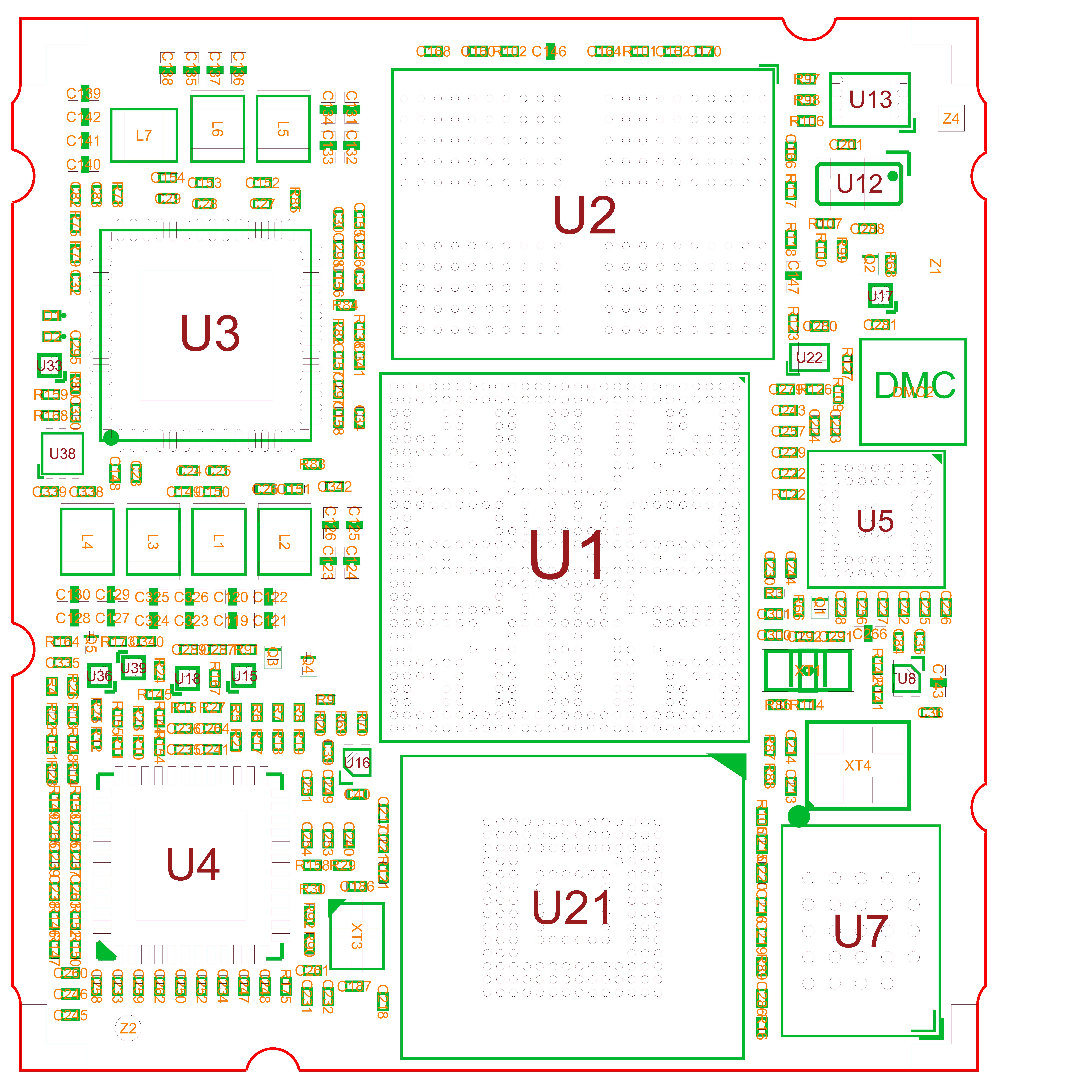
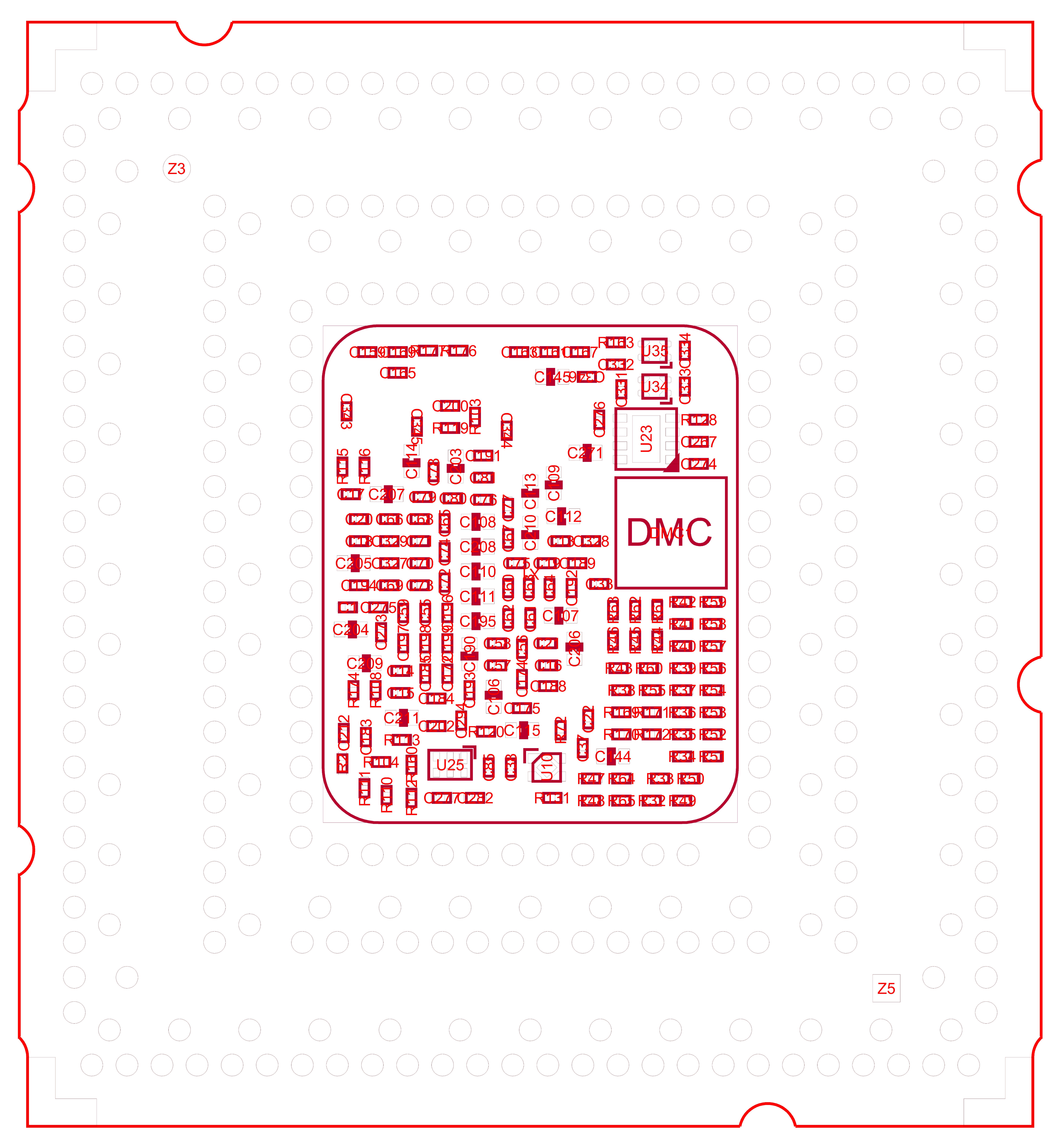
phyCORE-i.MX 8M Mini Component Placement
| Anchor | ||||
|---|---|---|---|---|
|
| Scroll Title | ||||
|---|---|---|---|---|
| ||||
...
| Scroll Title | ||||
|---|---|---|---|---|
| ||||
...
phyCORE-i.MX 8M Mini Minimal Operating Requirements
...
| Anchor | ||||
|---|---|---|---|---|
|
| Warning |
|---|
We recommend connecting all available VDD_3V3 input pins to the power supply system on a custom carrier board housing the phyCORE-i.MX 8M Mini and, at minimum, the matching number of GND pins neighboring the VDD_3V3 input pins. In addition, proper implementation of the phyCORE-i.MX 8M Mini module into a target application also requires connecting all GND pins. |
...
Pin Description
...
| Anchor | ||||
|---|---|---|---|---|
|
| Warning |
|---|
Module connections must not exceed their expressed maximum voltage or current. Maximum signal input values are indicated in the corresponding controller manuals/datasheets. As damage from improper connections varies according to use and application, it is the user 's responsibility to must take appropriate safety measures to ensure that the module connections are protected from overloading through connected peripherals. |
...
| Tip | ||
|---|---|---|
| ||
|
...
| Note | ||
|---|---|---|
| ||
Existing issues may be solved by referring to the following chapters in NXP Mask Set Errata for Mask 0N87W, Rev. 1, 09/2021:
It is good design practice to never rely on the SoC-internal pull resistors. |
...
| Scroll Indexterm | ||
|---|---|---|
|
Unused Signals
| Anchor | ||||
|---|---|---|---|---|
|
It is recommended to handle unused signals according to the table below:
...
The phyCORE‑i.MX 8M Mini operates off of a single power supply voltage. The following sections discuss the primary power pins on the phyCORE-i.MX 8M Mini Connector X1 in detail.
...
...
| secondary | Primary System Power (VDD_3V3) |
|---|---|
| primary | Power |
Primary System Power (VDD_3V3)
| Anchor | ||||
|---|---|---|---|---|
|
The phyCORE‑i.MX 8M Mini operates with a single primary voltage supply. Onboard switching and low dropout regulators generate the 2.5 V, 1.8 V, 1.2 V, 1.1 V, 0.9 V, and 0.8 V voltage rails required by the i.MX 8M Mini CPU and onboard components from the input voltage VDD_3V3.
...
| Warning | ||
|---|---|---|
| ||
As a general design rule, PHYTEC recommends connecting all GND pins neighboring signals which are being used in the application circuitry. For maximum EMI performance, all GND pins should be connected to a solid ground plane. |
...
Power Management IC (PMIC)(U3)
...
...
| Anchor | ||||
|---|---|---|---|---|
|
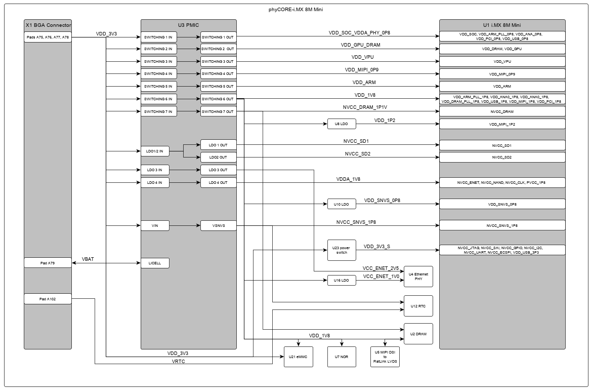
The phyCORE-i.MX 8M Mini provides an onboard Power Management IC (PMIC) at position U3 to generate different voltages required by the microcontroller and the onboard components. The L-862e.Ax phyCORE-i.MX 8M Mini/phyBOARD-Polis (1518.1a / 1532.1) HW Manual Head figure presents a graphical depiction of the powering scheme. The PMIC supports many functions like on-chip RTC and different power management functionalities like dynamic voltage control, different low power modes, and regulator supervision. It is connected to the i.MX 8M Mini via the onboard I2C bus (I2C1) (L-862e.Ax phyCORE-i.MX 8M Mini/phyBOARD-Polis (1518.1a / 1532.1) HW Manual Head). The I2C address of the PMIC is 0x08.
...
...
Power Domains
...
...
| Anchor | ||||
|---|---|---|---|---|
|
| Anchor | ||||
|---|---|---|---|---|
|
| Scroll Title | ||||
|---|---|---|---|---|
| ||||
...
| Scroll Title | ||||||||||||||||||||||||||||||||||||||||||||||
|---|---|---|---|---|---|---|---|---|---|---|---|---|---|---|---|---|---|---|---|---|---|---|---|---|---|---|---|---|---|---|---|---|---|---|---|---|---|---|---|---|---|---|---|---|---|---|
| ||||||||||||||||||||||||||||||||||||||||||||||
|
...
...
External Logic Supply Voltage
...
...
| Anchor | ||||
|---|---|---|---|---|
|
The voltage level of the phyCORE’s logic circuitry is VDD_3V3_S (3.3 V) which is derived from the SOM main input voltage, VDD_3V3. In order to follow the mandatory power-up and power-down sequencing for the i.MX 8M Mini, external devices have to be supplied by the I/O supply voltage VDD_3V3_S which is brought out at pin E14 of the phyCORE-Connector. The use of VDD_3V3_S ensures that external components are only supplied when the supply voltages of the i.MX 8M Mini are stable.
...
| Tip | ||
|---|---|---|
| ||
If used to control or supply bus switches on the phyCORE side, VDD_3V3_S separates the supply voltages generated on the phyCORE‑i.MX 8M Mini and the supply voltages used on the carrier board/custom application. This way, voltages at the IO pins of the phyCORE-i.MX 8M Mini which are sourced from the supply voltage of peripheral devices attached to the SOM are avoided. These voltages can cause a current flow into the controller, especially if peripheral devices attached to the interfaces of the i.MX 8M Mini are supposed to be powered while the phyCORE‑i.MX 8M Mini is in suspend mode or turned off. The bus switches can be supplied by VDD_3V3_S on the phyCORE side, or the bus switches' output enabled to the SOM can be controlled by X_PGOOD to prevent these voltages from occurring. The use of level shifters supplied with VDD_3V3_S allows the signals to be converted according to the needs of the custom target hardware. Alternatively, signals can be connected to an open drain circuitry with a pull-up resistor attached to VDD_3V3_S. |
...
Backup Power (VBAT)
...
| Anchor | ||||
|---|---|---|---|---|
|
At pin A79 (Signal VBAT) of the phyCORE-i.MX 8M Mini, a secondary 3.3 V voltage source may be attached to the SOM. The PMIC (U3) will use this secondary source to generate NVCC_SNVS_1P8 in case VDD_3V3 falls below a value of approx. 2.8 V.
...
On-Board RTC and RTC Backup Power (VRTC)
...
| Anchor | ||
|---|---|---|
|
...
|
At pin A102 (Signal VRTC) of the phyCORE-i.MX 8M Mini, a secondary voltage source may be attached to the SOM in order to buffer the onboard RTC U12, while the SOM input voltage is not present. This manual describes only one of the available RTC active power states, which is used in conjunction with the phyBOARD-POLIS and the phyCORE-i.MX 8M Mini. The RTC RV-3028-C7 will enter its backup mode as soon as it detects the voltage level at Pin VRTC to be higher than the SOM input voltage VDD_3V3.
...
| Warning | ||
|---|---|---|
| ||
In its backup power state, the RTC will cease to communicate over I2C1 if the voltage level at the Pin VRTC is higher than the SOM input voltage VDD_3V3. In order to avoid unnecessary problems, the recommended voltage difference between VDD_3V3 and VRTC is approx. 300 mV. |
...
| Scroll Indexterm | ||
|---|---|---|
|
Reset
| Anchor | ||||
|---|---|---|---|---|
|
Pin C43 on the phyCORE-Connector is designated as an open-drain reset input with a pull-up resistor, that triggers a hard reset of the module. The external reset signal is connected to the enable signal of the voltage supervisor U41, which triggers a watchdog event in the PMIC resulting in a hard reset of the module. For debouncing purposes, the U41 delays the signal by 8,804 ms.
For PCB version versions 1518.0, 1518.1a and 1518.2 additional precautions have to be taken regarding the undervoltage detection of the phyCORE-i.MX 8M Mini. X_nPOR_IN must be held on a logical low level, as long as VDD_3V3 is below 3.135 V. If this is not considered in the design of a baseboard, there is a small chance , that the SoM could enter an unspecified mode of operation. PCB version 1518.3 and higher will not require this feature any longer, yet it is good engineering practice, to monitor all voltage rails at all times.
...
System Boot Configuration
| Anchor | |||
|---|---|---|---|
|
...
...
|
...
|
i.MX 8M Mini System Boot Settings
Most features of the i.MX 8M Mini microcontroller are configured and/or programmed during the initialization routine. Essential boot features however are latched into i.MX 8M Mini registers from pre-configured pull-resistors following power-on reset (POR_B) de-assertion.
The latched-in information includes:
- Boot mode selection
- Boot device selection
- Detailed boot device configuration
The internal ROM code is the first code executed during the initialization process of the i.MX 8M Mini after POR de-assertion. The ROM code detects the boot mode through pins X_BOOT_MODE0 and X_BOOT_MODE1, while the boot device is selected and configured by determining the state of the eFUSEs and/or the corresponding GPIO pins (BOOT_CFGx[14:12]).
...
Boot Mode Selection
...
| Anchor | ||||
|---|---|---|---|---|
|
The i.MX 8M Mini boot mode is determined by the logical levels of the pins X_BOOT_MODE0 and X_BOOT_MODE1 approx. 31 µs after POR_B de-assertion. X_BOOT_MODE0 and X_BOOT_MODE1 are brought out at the phyCORE‑Connector pins C15 and C16. Possible settings and the resulting boot configuration of the i.MX 8M Mini are described in the following table:Anchor phyCORE-i.MX 8M Mini Boot Modes phyCORE-i.MX 8M Mini Boot Modes
...
In fuse boot and internal boot mode, the ROM code finds the bootloader in permanent memories, such as eMMC or SD-Cards, and executes it. The boot device selection and the required interface configuration are accomplished with the help of the eFUSEs and/or the corresponding GPIO input.
...
Boot
...
Device Selection and
...
Configuration
...
| Anchor | ||||
|---|---|---|---|---|
|
In fuse boot and internal boot mode, the ROM code uses the BOOT_CFG pin states and eFUSEs to determine the boot device and its detailed configuration.
...
| Scroll Title | ||||||||||||||||||||||||||||||||||||||||||||||||||||||||||||||||||||||||||||||||||||||||||||||||||||||||||||||||||||||||||||||||||||
|---|---|---|---|---|---|---|---|---|---|---|---|---|---|---|---|---|---|---|---|---|---|---|---|---|---|---|---|---|---|---|---|---|---|---|---|---|---|---|---|---|---|---|---|---|---|---|---|---|---|---|---|---|---|---|---|---|---|---|---|---|---|---|---|---|---|---|---|---|---|---|---|---|---|---|---|---|---|---|---|---|---|---|---|---|---|---|---|---|---|---|---|---|---|---|---|---|---|---|---|---|---|---|---|---|---|---|---|---|---|---|---|---|---|---|---|---|---|---|---|---|---|---|---|---|---|---|---|---|---|---|---|---|
| ||||||||||||||||||||||||||||||||||||||||||||||||||||||||||||||||||||||||||||||||||||||||||||||||||||||||||||||||||||||||||||||||||||
|
...
...
i.MX 8M Nano System Boot Settings
| Anchor | ||||
|---|---|---|---|---|
|
The i.MX 8M Nano uses a boot process different from the i.MX 8M Mini. Boot devices with fixed configuration may be selected through the use of 6 Boot Mode pins, 2 of which are shared with the i.MX 8M Mini. The phyCORE-i.MX 8M Nano is pre-configured with the default Boot Mode setting eMMC boot.
...
Cite summary showCitationLinks false local true
...
LPDDR4-RAM (U2)
...
| Anchor | ||||
|---|---|---|---|---|
|
The RAM memory of the phyCORE‑i.MX 8M Mini is comprised of one 32-bit wide bank with two 16-bit wide LPDDR4-RAM chips in one integrated circuit. The chips are connected to the DDR interface called the DDR Controller (DDRC) of the i.MX 8M Mini microcontroller.
Typically, the LPDDR4-RAM initialization is performed by a boot loader or operating system following a power-on reset and must not be changed at a later point by any application code. When writing custom code independent of an operating system or boot loader, the RAM must be initialized by accessing the appropriate RAM configuration registers on the i.MX 8M Mini controller. Refer to the NXP i.MX 8M Mini Reference Manual for accessing and configuring these registers.
...
...
QUAD SPI-NOR (U7)
| Anchor | ||||
|---|---|---|---|---|
|
The Quad NOR flash memory at U7 is connected to the Flexible Serial Peripheral Interface A (FlexSPI A). The connected flash device uses the provided Chip Select 0 signal (QSPIA_SS0). The NOR flash device is powered by the 1.8 V supply voltage VDD_1V8. No further voltages are required to program the device.
...
For more information about the NOR Flash, please refer to the NXP i.MX 8M Mini Reference Manual.
...
eMMC Flash Memory (U21)
...
...
| Anchor | ||||
|---|---|---|---|---|
|
The managed NAND (eMMC) flash device is powered by the supply voltages VDD_1V8 (1.8 V) and VDD_3V3_S (3.3 V). No further voltages are required for programming the device. The eMMC memory is connected to the SDIO3 interface of the i.MX 8M Mini. Any parts that are footprint (BGA153) and functionally compatible may be used with the phyCORE-i.MX 8M Mini.
For more information about the eMMC, please refer to the NXP i.MX 8M Mini Reference Manual.
...
| Scroll Indexterm | ||||
|---|---|---|---|---|
|
I2C EEPROM (U13)
| Anchor | ||||
|---|---|---|---|---|
|
The phyCORE‑i.MX 8M Mini is populated with a 4 kB I2C
...
| Cite summary | ||||
|---|---|---|---|---|
|
...
EEPROM Write Control
...
...
| Anchor | ||||
|---|---|---|---|---|
|
The Write Control (WC) signal of the EEPROM is permanently fixed to GND over resistor R106, so the EEPROM is not always write-protected.
...
The following sections detail each of these serial interfaces.
...
...
SDIO Interfaces
...
Anchor SDIO Interfaces SDIO Interfaces
| SDIO Interfaces | |
| SDIO Interfaces |
The SDIO interfaces are part of the ultra Secured Digital Host Controller and can be used to connect external SD-Cards, eMMC, or any other device requiring an SDIO interface (examples include WiFI, I/O expansion). The phyCORE‑i.MX 8M Mini features two SDIO interfaces (4 and 8-Bit). On the phyCORE‑i.MX 8M Mini, the interface signals extend from the controller's first and second Ultra Secured Digital Host Controller (uSDHC1/uSDHC2) to the phyCORE-Connector.
uSDHC2 provides dedicated card-detect, write-protect and power enable signals. For uSDHC2 to function a pull-up resistor (eg. 10k) from X_SD2_PWR_EN to the SOM input voltage VDD_3V3 is required. This enables the uSDHC2 interface by powering the corresponding domain in the i.MX 8M Mini. This feature may be used to limit access to the CPU through an openly available SD-Card slot, or for similar purposes.
uSDHC1 card-detect and write-protect functions may be implemented by using GPIOs of the i.MX 8M Mini. Refer to the NXP i.MX 8M Mini Reference Manual. For more information about SD-Cards, please refer to the manufacturer's user manual.
...
| Scroll Title | ||||||||||||||||||||||||||||||||||||||||||||||||||||||||||||||||||||||||||||||||||||||
|---|---|---|---|---|---|---|---|---|---|---|---|---|---|---|---|---|---|---|---|---|---|---|---|---|---|---|---|---|---|---|---|---|---|---|---|---|---|---|---|---|---|---|---|---|---|---|---|---|---|---|---|---|---|---|---|---|---|---|---|---|---|---|---|---|---|---|---|---|---|---|---|---|---|---|---|---|---|---|---|---|---|---|---|---|---|---|
| ||||||||||||||||||||||||||||||||||||||||||||||||||||||||||||||||||||||||||||||||||||||
|
...
...
...
Universal Asynchronous Interface
...
| Anchor | ||||
|---|---|---|---|---|
|
The phyCORE‑i.MX 8M Mini provides four high-speed universal asynchronous interfaces. Hardware flow control (RTS and CTS signals) may be implemented through the use of additional GPIO signals. See muxing options in NXP i.MX 8M Mini Reference Manual for more information. Location of the signals on the phyCORE-Connector:Anchor UART Signals UART Signals
| Scroll Title | ||||||||||||||||||||||||||||||||||||||||||||||||||||||||||||||||||||||||||
|---|---|---|---|---|---|---|---|---|---|---|---|---|---|---|---|---|---|---|---|---|---|---|---|---|---|---|---|---|---|---|---|---|---|---|---|---|---|---|---|---|---|---|---|---|---|---|---|---|---|---|---|---|---|---|---|---|---|---|---|---|---|---|---|---|---|---|---|---|---|---|---|---|---|---|
| ||||||||||||||||||||||||||||||||||||||||||||||||||||||||||||||||||||||||||
|
...
USB OTG Interfaces
| Anchor | ||||
|---|---|---|---|---|
|
The phyCORE‑i.MX 8M Mini provides two high-speed USB OTG interfaces, which use the i.MX 8M Mini’s embedded High-Speed USB 2.0 PHY.
...
| Scroll Title | ||||||||||||||||||||||||||||||||||||||||||||||||||
|---|---|---|---|---|---|---|---|---|---|---|---|---|---|---|---|---|---|---|---|---|---|---|---|---|---|---|---|---|---|---|---|---|---|---|---|---|---|---|---|---|---|---|---|---|---|---|---|---|---|---|
| ||||||||||||||||||||||||||||||||||||||||||||||||||
|
...
...
Ethernet Interface
...
...
| Anchor | ||||
|---|---|---|---|---|
|
Connection of the phyCORE‑i.MX 8M Mini to the World Wide Web or a local area network (LAN) is possible using the onboard GbE PHY at U4. It is connected to the RGMII interface of the i.MX 8M Mini. The PHY operates with a data transmission speed of 10, 100, or 1000 Mbit/s. Alternatively, the RGMII interface which is available on the phyCORE‑Connector can be used to connect an external PHY. In this case, the onboard GbE PHY (U4) must not be populated (see L-862e.Ax phyCORE-i.MX 8M Mini/phyBOARD-Polis (1518.1a / 1532.1) HW Manual Head).
...
Ethernet
...
PHY (U4)
...
...
| Anchor | ||||
|---|---|---|---|---|
|
With an Ethernet PHY mounted at U4, the phyCORE‑i.MX 8M Mini has been designed for use in 10/100/1000Base-T networks. The 10/100/1000Base-T interface with its LED signals extends to the phyCORE-i.MX 8M Mini Connector X1.
...
Connection to external Ethernet magnetics should be done using very short signal traces. The A+/A-, B+/B-, C+/C-, and D+/D- signals should be routed as 100 Ohm differential pairs. The same applies to the signal lines after the transformer circuit. The carrier board layout should avoid any other signal lines crossing the Ethernet signals.
...
| Scroll Indexterm | ||||||
|---|---|---|---|---|---|---|
|
...
Ethernet PHY Reset
| Anchor | ||||
|---|---|---|---|---|
|
The Ethernet PHY at U4 can be reset via software. The reset input of the Ethernet PHY is connected to the Power-On Reset (POR) signal of the module and to the GPIO RESET_ETHPHY of the i.MX 8M Mini.
...
MAC Address
...
...
| Anchor | ||||
|---|---|---|---|---|
|
In a computer network such as a local area network (LAN), the MAC (Media Access Control) address is a unique computer hardware number. For a connection to the internet, a table is used to convert the assigned IP number to the hardware’s MAC address. In order to guarantee that the MAC address is unique, all addresses are managed in a central location. PHYTEC has acquired a pool of MAC addresses. The MAC address of the phyCORE‑i.MX 8M Mini is located on the bar code sticker attached to the module. This number is a 12-digit HEX value.
...
...
RGMII Interface
| Anchor | ||||
|---|---|---|---|---|
|
In order to use an external Ethernet PHY instead of the onboard GbE PHY at U8, the RGMII interface (ENET) of the i.MX 8M Mini is brought out at phyCORE-i.MX 8M Mini Connector X1.
| Note | ||
|---|---|---|
| ||
Existing issues may be solved by referring to the following chapters in NXP Mask Set Errata for Mask 0N87W, Rev. 1, 09/2021:
|
...
| Scroll Title | ||||||||||||||||||||||||||||||||||||||||||||||||||||||||||||||||||||||||||||||||||||||||||||||||||||||||||||||
|---|---|---|---|---|---|---|---|---|---|---|---|---|---|---|---|---|---|---|---|---|---|---|---|---|---|---|---|---|---|---|---|---|---|---|---|---|---|---|---|---|---|---|---|---|---|---|---|---|---|---|---|---|---|---|---|---|---|---|---|---|---|---|---|---|---|---|---|---|---|---|---|---|---|---|---|---|---|---|---|---|---|---|---|---|---|---|---|---|---|---|---|---|---|---|---|---|---|---|---|---|---|---|---|---|---|---|---|---|---|---|
| ||||||||||||||||||||||||||||||||||||||||||||||||||||||||||||||||||||||||||||||||||||||||||||||||||||||||||||||
|
...
...
SPI Interfaces
| Anchor | ||||
|---|---|---|---|---|
|
The Serial Peripheral Interface (SPI) interface is a four-wire, bidirectional serial bus that provides a simple and efficient method for data exchange among devices. The phyCORE provides two SPI interfaces on the phyCORE‑i.MX 8M Mini Connector X1.
...
| Note | ||
|---|---|---|
| ||
Existing issues may be solved by refering referring to the following chapters in NXP Mask Set Errata for Mask 0N87W, Rev. 1, 09/2021:
|
...
| Scroll Title | ||||||||||||||||||||||||||||||||||||||||||||||||||
|---|---|---|---|---|---|---|---|---|---|---|---|---|---|---|---|---|---|---|---|---|---|---|---|---|---|---|---|---|---|---|---|---|---|---|---|---|---|---|---|---|---|---|---|---|---|---|---|---|---|---|
| ||||||||||||||||||||||||||||||||||||||||||||||||||
|
...
...
| secondary | I2C Interface |
|---|---|
| primary | Serial Interfaces |
I2C Interface
| Anchor | ||||
|---|---|---|---|---|
|
The Inter-Integrated Circuit (I2C) interface is a two-wire, bidirectional serial bus that provides a simple and efficient method for data exchange among devices. The i.MX 8M Mini contains four identical, independent Multimaster fast-mode I2C modules. The interface of three modules is available at the phyCORE-Connector. The first I2C module (I2C1) connects to the onboard EEPROM at U13 (I2C EEPROM), the PMIC at U3 (Power Management IC), the Real-Time Clock at U12, and the MIPI to LVDS converter at U5 L-862e.Ax phyCORE-i.MX 8M Mini/phyBOARD-Polis (1518.1a / 1532.1) HW Manual Head. The MIPI to LVDS converter connects to the I2C1 interface through the level shifter U22. The voltage domain in this part of the bus is 1,8 V.
...
| Scroll Title | ||||||||||||||||||||||||||||||||||||||
|---|---|---|---|---|---|---|---|---|---|---|---|---|---|---|---|---|---|---|---|---|---|---|---|---|---|---|---|---|---|---|---|---|---|---|---|---|---|---|
| ||||||||||||||||||||||||||||||||||||||
|
...
...
Onboard I2C Bus
...
| Anchor | ||
|---|---|---|
|
...
|
The first I2C module (I2C1) connects to the onboard EEPROM at U13 and the PMIC at U3. The following table shows the addresses of all I2C1 devices on the phyCORE-i.MX 8M Mini:
| Anchor | ||||
|---|---|---|---|---|
|
| Scroll Title | ||||||||||||||||||||||||||||||
|---|---|---|---|---|---|---|---|---|---|---|---|---|---|---|---|---|---|---|---|---|---|---|---|---|---|---|---|---|---|---|
| ||||||||||||||||||||||||||||||
|
...
Synchronous Audio Interface (SAI)
| Anchor | ||||
|---|---|---|---|---|
|
The phyCORE-i.MX 8M Mini features a Synchronous Audio Interface that supports full-duplex serial interfaces with frame synchronization such as I2S, AC97, and TDM. The interface is divided into four sub-interfaces: SAI1, SAI2, SAI3, and SAI5. All signals are routed directly to the phyCORE-i.MX 8M Mini Connector X1. All signals are part of the VDD_3V3_S voltage domain.
...
| Note | ||
|---|---|---|
| ||
Existing issues may be solved by refering referring to the following chapters in NXP Mask Set Errata for Mask 0N87W, Rev. 1, 09/2021:
|
...
| Scroll Title | ||||||||||||||||||||||||||||||||||||||||||||||||||||||||||||||||||||
|---|---|---|---|---|---|---|---|---|---|---|---|---|---|---|---|---|---|---|---|---|---|---|---|---|---|---|---|---|---|---|---|---|---|---|---|---|---|---|---|---|---|---|---|---|---|---|---|---|---|---|---|---|---|---|---|---|---|---|---|---|---|---|---|---|---|---|---|---|
| ||||||||||||||||||||||||||||||||||||||||||||||||||||||||||||||||||||
|
...
...
PCI Express Interface
| Anchor | ||||
|---|---|---|---|---|
|
The 1-lane PCI Express interface of the phyCORE‑i.MX 8M Mini provides PCIe Gen. 2.0 functionality which supports 5 Gbit/s operations. Furthermore, the interface is fully backward compatible with the 2.5 Gbit/s Gen. 1.1 specification. Additional control signals which might be required (e.g. “present” and “wake”) can be implemented via the use of GPIOs. Please refer to the schematic of a suitable PHYTEC carrier board (e.g. phyBOARD‑Polis) for a circuit example. The table below show the signal location for the PCIe interface.Anchor PCIe Signals PCIe Signals
| Note | ||
|---|---|---|
| ||
Existing issues may be solved by refering referring to the following chapters in NXP Mask Set Errata for Mask 0N87W, Rev. 1, 09/2021:
|
...
| Scroll Title | ||||||||||||||||||||||||||||||||||||||||||||||||||||||||||||||
|---|---|---|---|---|---|---|---|---|---|---|---|---|---|---|---|---|---|---|---|---|---|---|---|---|---|---|---|---|---|---|---|---|---|---|---|---|---|---|---|---|---|---|---|---|---|---|---|---|---|---|---|---|---|---|---|---|---|---|---|---|---|---|
| ||||||||||||||||||||||||||||||||||||||||||||||||||||||||||||||
|
...
...
General Purpose I/Os
...
| Anchor | ||||
|---|---|---|---|---|
|
The following table lists all pins not used by any of the other interfaces described explicitly in this manual and which, therefore, can be used as GPIO without harming other features of the phyCORE‑i.MX 8M Mini. In addition, most pins directly routed to the phyCORE-i.MX M Mini Connector X1 can be configured as GPIO due to the multiplexing functionality of the i.MX 8M Mini.
...
| Scroll Title | ||||||||||||||||||||||||||||||||||||||||||||||||||||||||||||||||||||
|---|---|---|---|---|---|---|---|---|---|---|---|---|---|---|---|---|---|---|---|---|---|---|---|---|---|---|---|---|---|---|---|---|---|---|---|---|---|---|---|---|---|---|---|---|---|---|---|---|---|---|---|---|---|---|---|---|---|---|---|---|---|---|---|---|---|---|---|---|
| ||||||||||||||||||||||||||||||||||||||||||||||||||||||||||||||||||||
|
...
JTAG Interface
| Anchor | ||||
|---|---|---|---|---|
|
The phyCORE‑i.MX 8M Mini is equipped with a JTAG interface for downloading program code into the external flash, internal controller RAM, or for any debugging programs that are executed. Location of the JTAG pins on the phyCORE-i.MX 8M Mini Connector X1:
...
| Warning | ||
|---|---|---|
| ||
It is not possible to use both an LVDS and MIPI display at the same time. Only one type of display can be used at any given time. |
...
LVDS (Flatlink)
...
...
| Anchor | ||||
|---|---|---|---|---|
|
The LVDS interface of the phyCORE-i.MX 8M Mini, using an optional MIPI to LVDS converter, is converted from the i.MX 8M Mini’s MIPI-DSI2 interface. The converter supports resolutions of up to 1920x1200 (WUXGA) at 60 frames per second with 24 bpp and reduced blanking. It is also suitable for resolutions of 1366x768 with 60 frames per second and 1280x800 at 60 frames per second, both 18 and 24 bpp. The LVDS interface is available only when U5 is mounted. Please refer to the Texas Instruments SN65DSI83 datasheet for more information.
...
| Scroll Title | ||||||||||||||||||||||||||||||||||||||||||||||||||||||||||||||||||||||||||||||||||||||
|---|---|---|---|---|---|---|---|---|---|---|---|---|---|---|---|---|---|---|---|---|---|---|---|---|---|---|---|---|---|---|---|---|---|---|---|---|---|---|---|---|---|---|---|---|---|---|---|---|---|---|---|---|---|---|---|---|---|---|---|---|---|---|---|---|---|---|---|---|---|---|---|---|---|---|---|---|---|---|---|---|---|---|---|---|---|---|
| ||||||||||||||||||||||||||||||||||||||||||||||||||||||||||||||||||||||||||||||||||||||
|
...
...
MIPI-Display Serial Interface 2 (MIPI-DSI2)
...
| Anchor | ||||
|---|---|---|---|---|
|
The i.MX 8M Mini’s MIPI-DSI2 interface provides resolutions of up to 1920x1080 at 60 frames per second. It uses four data channels and one clock channel. The MIPI-DSI2 interface is only available if the MIPI to LVDS converter U5 is not mounted. The interface provides a maximum bit rate of 1,5 Gbit/s.
| Scroll Title | ||||||||||||||||||||||||||||||||||||||||||||||||||||||||||||||||||||||||||||||||||||||
|---|---|---|---|---|---|---|---|---|---|---|---|---|---|---|---|---|---|---|---|---|---|---|---|---|---|---|---|---|---|---|---|---|---|---|---|---|---|---|---|---|---|---|---|---|---|---|---|---|---|---|---|---|---|---|---|---|---|---|---|---|---|---|---|---|---|---|---|---|---|---|---|---|---|---|---|---|---|---|---|---|---|---|---|---|---|---|
| ||||||||||||||||||||||||||||||||||||||||||||||||||||||||||||||||||||||||||||||||||||||
|
...
...
MIPI CSI-2 Camera Interface
| Anchor | ||||
|---|---|---|---|---|
|
The phyCORE-i.MX 8M Mini features a MIPI CSI-2 camera interface. It is routed directly to the phyCORE-i.MX 8M Mini Connector X1. The interface provides a maximum bit rate of 1,5 Gbit/s. It uses four data channels and one clock channel. All signals, including control signals and an I2C interface, to use the camera interfaces, according to PHYTEC's phyCAM‑S standard, are available at the phyCORE‑i.MX 8M Mini Connector.
...
| Scroll Title | ||||||||||||||||||||||||||||||||||||||||||||||||||||||||||||||||||||||||||||||||||||||
|---|---|---|---|---|---|---|---|---|---|---|---|---|---|---|---|---|---|---|---|---|---|---|---|---|---|---|---|---|---|---|---|---|---|---|---|---|---|---|---|---|---|---|---|---|---|---|---|---|---|---|---|---|---|---|---|---|---|---|---|---|---|---|---|---|---|---|---|---|---|---|---|---|---|---|---|---|---|---|---|---|---|---|---|---|---|---|
| ||||||||||||||||||||||||||||||||||||||||||||||||||||||||||||||||||||||||||||||||||||||
|
...
...
...
SPDIF Interface
...
...
| Anchor | ||||
|---|---|---|---|---|
|
The phyCORE-i.MX 8M Mini features a SPDIF interface. It is routed directly to the phyCORE-i.MX 8M Mini Connector X1.
| Note | ||
|---|---|---|
| ||
Existing issues may be solved by refering referring to the following chapters in NXP Mask Set Errata for Mask 0N87W, Rev. 1, 09/2021:
|
...
| Scroll Title | |||||||||||||||||||||||||||||||||||||||||||
|---|---|---|---|---|---|---|---|---|---|---|---|---|---|---|---|---|---|---|---|---|---|---|---|---|---|---|---|---|---|---|---|---|---|---|---|---|---|---|---|---|---|---|---|
| |||||||||||||||||||||||||||||||||||||||||||
|
...
CPU Core Frequency Scaling
| Anchor | ||||
|---|---|---|---|---|
|
The i.MX 8M Mini on the phyBOARD‑Polis is able to scale the clock frequency and voltage. This is used to save power when the full performance of the CPU is not needed. Scaling the frequency and voltage is referred to as Dynamic Voltage and Frequency Scaling (DVFS).
...
These specifications describe the standard configuration of the phyCORE‑i.MX 8M Mini as of the printing of this manual.
...
.
...
...
phyCORE-i.MX 8M Mini Power Consumption
| Anchor | ||||
|---|---|---|---|---|
|
In order to illustrate the power consumption of the phyCORE-i.MX 8M Mini in various realistic load scenarios, multiple measurements were conducted. It is important to note, that these measurements are a sole depiction of the specific stresses, asserted to the SOM through the specified software applications. The given results may be utilized to dimension a power supply for the phyCORE-i.MX 8M Mini on custom hardware. Especially custom software may yield different results in power consumption compared to the values posted in the table below. It is vital that power consumption of the phyCORE-i.MX 8M Mini is evaluated when it is intended to be used with custom software.
...
| Tip | ||
|---|---|---|
| ||
For further information and assistance regarding your application's power consumption, please contact PHYTEC sales. |
...
Low-
...
Power Modes
...
Anchor Product Temperature Grades Product Temperature Grades
| Product Temperature Grades | |
| Product Temperature Grades |
The i.MX 8M Mini offers various low-power modes. For further, more detailed information, on how to activate and utilize the different low-power modes please refer to the PHYTEC phyCORE-i.MX 8M Mini BSP Manual and NXP i.MX 8M Mini Reference Manual. The phyCORE-i.MX 8M Mini supports the following low-power modes:
-
-
-
...
Product Temperature GradesAnchor
...
Product Temperature Grades
| Product Temperature Grades |
...
Product Temperature Grades
| Product Temperature Grades |
| Warning | ||
|---|---|---|
| ||
The right temperature grade of the module greatly depends on the use case. It is necessary to determine if the use case suits the temperature range of the chosen module (see below). If necessary, a heat spreader can be used for temperature compensation. |
...
| Scroll Title | ||||||||||||||||||||||||||||||||
|---|---|---|---|---|---|---|---|---|---|---|---|---|---|---|---|---|---|---|---|---|---|---|---|---|---|---|---|---|---|---|---|---|
| ||||||||||||||||||||||||||||||||
|
...
...
phyCORE-i.MX 8M Mini BGA Mounting
| Anchor | ||||
|---|---|---|---|---|
|
The phyCORE i.MX 8M Mini uses Ball Grid Array (BGA) to mount to a carrier board (for example, phyBOARD-Polis). BGA provides several advantages:
...
Hints for Integrating and Handling the phyCORE‑i.MX 8M Mini
...
...
Integrating the phyCORE-i.MX 8M Mini
...
| Anchor | ||||
|---|---|---|---|---|
|
Apart from this hardware manual, more information is available to facilitate the integration of the phyCORE‑i.MX 8M Mini into customer applications.
- The design of the phyBOARD‑Polis can be used as a reference for any customer application.
- Many answers to common questions can be found at: https://www.phytec.de/produkt/system-on-modules/phycore-imx-8m-mini-nano/ or https://www.phytec.eu/product-eu/system-on-modules/phycore-imx-8m-mini-nano/
- The link “Carrier Board” within the category Dimensional Drawing leads to the layout data as shown in L-862e.Ax phyCORE-i.MX 8M Mini/phyBOARD-Polis (1518.1a / 1532.1) HW Manual Head. It is available in different file formats. The use of this data allows the user to integrate the phyCORE-i.MX 8M Mini SOM as a single component of your design.
- Different support packages are available for support in all stages of embedded development. Please visit http://www.phytec.de/de/support/support-pakete.html or https://www.phytec.eu/support/support-packages/ or contact our sales team for more details.
- Many answers to common questions can be found at:
https://www.phytec.de/produkt/system-on-modules/phycore-imx-8m-mini-nano/
or
https://www.phytec.eu/product-eu/system-on-modules/phycore-imx-8m-mini-nano/
...
Integrating the phyCORE
...
into a Target Application
...
Successful integration in user target circuitry greatly depends on the adherence to the layout design rules for the GND connections of the phyCORE module. For maximum EMI performance, PHYTEC recommends, as a general design rule, connecting all GND pins to a solid ground plane. As a minimum, all GND pin neighboring signals which are being used in the application circuitry should be connected to GND.
...
Handling the phyCORE-i
...
.MX 8M Mini
...
| Anchor | ||||
|---|---|---|---|---|
|
...
|
phyCORE Module Modifications
The removal of various components, such as the microcontroller or the standard quartz, is not advisable given the compact nature of the module. Should this nonetheless be necessary, please ensure that the board, as well as surrounding components and sockets, remain undamaged while desoldering. Overheating the board can cause the solder pads to loosen, rendering the module inoperable. If soldered components need to be removed, the use of a desoldering pump, desoldering braid, an infrared desoldering station, desoldering tweezers, hot air rework stations, or other desoldering methods is strongly recommended. Follow the instructions carefully for whatever method of removal is used.
...
phyCORE-i.MX 8M Mini on the phyBOARD-Polis
| Anchor | ||||
|---|---|---|---|---|
|
...
Hardware Overview
...
| Anchor | ||||
|---|---|---|---|---|
|
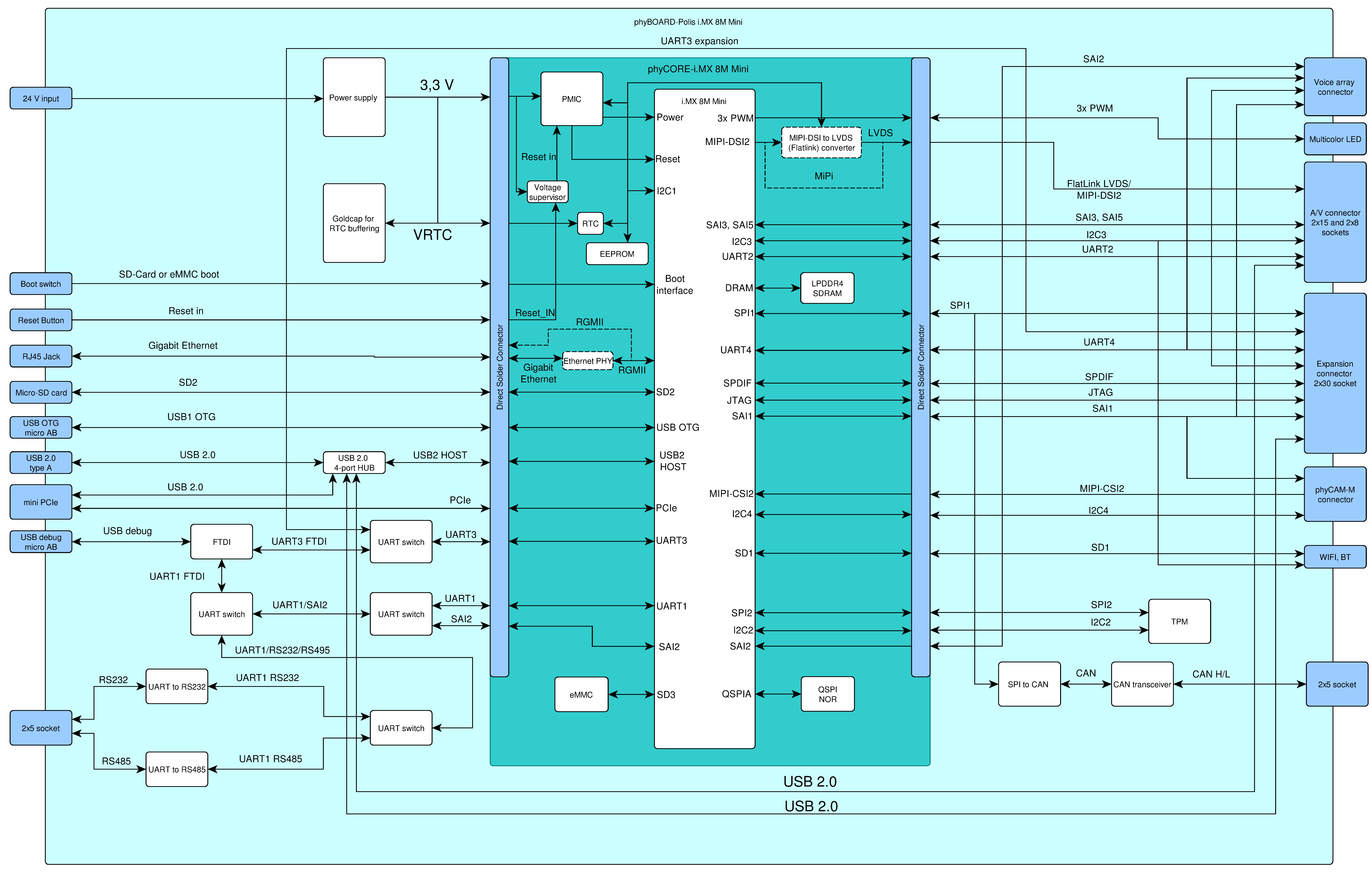
The phyBOARD‑Polis for phyCORE-i.MX 8M Mini is a low-cost, feature-rich software development platform supporting the NXP Semiconductors i.MX 8M Mini microcontroller. Due to numerous standard interfaces, the phyBOARD‑Polis can serve as the bedrock for any application. At the core of the phyBOARD‑Polis is the PCL-069/phyCORE-i.MX 8M Mini System On Module (SOM) containing the processor, DRAM, eMMC, power regulation, supervision, transceivers, and other core functions required to support the i.MX 8M Mini processor. Surrounding the SOM is the PB-02820-xxxxx.Ax/phyBOARD‑Polis carrier board, adding power input, buttons, connectors, signal breakout, and Ethernet connectivity along with other peripherals.
The PCL-069 System On Module connects to the phyBOARD‑Polis carrier board using a Ball Grid Array (BGA). The PCL-069 SOM is soldered directly onto the phyBOARD‑Polis using PHYTEC's Direct Solder Connect technology. This solution offers an ultra-low-cost Single Board Computer for the i.MX 8M Mini processor, while maintaining most of the advantages of the SOM concept.
...
phyBOARD-
...
Polis Concept
...
| Anchor | ||
|---|---|---|
|
...
|
phyCORE carrier boards are designed and tested to be used in:
- series products
- evaluating, testing, and prototyping PHYTEC System on Modules in laboratory environments prior to their use in customer-designed applications.
PHYTEC phyCORE carrier boards are fully equipped with all mechanical and electrical components necessary for a fast, secure start-up. Subsequent communication to and programming of applicable PHYTEC System on Modules (SOM) is made easy.
...
- The phyCORE-i.MX 8M Mini module populated with the i.MX 8M Mini microprocessor and all applicable SOM circuitry such as LPDDR 4 SDRAM, managed NAND, Ethernet transceiver, WiFi, and PMIC to name a few.
- The phyBOARD-Polis carrier board offers all essential components and connectors for a start-up including a power supply for 24 V input voltage, and interface connectors such as USB micro-AB, USB A, and Ethernet RJ-45 which enable the use of the SOM’s interfaces with standard cables.
The carrier board can also serve as a reference design for the development of custom target hardware in which the phyCORE SOM is deployed. Carrier board schematics are available under a Non-Disclosure Agreement (NDA). Reuse of carrier board circuitry enables users of PHYTEC SOMs to shorten time-to-market, reduce development costs, and avoid substantial design issues and risks.
...
SBCplus Concept
...
Anchor SBCplus Concept SBCplus Concept
| SBCplus Concept | |
| SBCplus Concept |
The SBCplus concept was developed to meet the many, small differences in customer requirements with little development effort. This greatly reduces the time to market. The core of the SBCplus concept is the SBC design library (a kind of construction set) that consists of a large number of function blocks (so-called "building blocks") that are continuously being refined and updated.
...
| Tip | ||
|---|---|---|
| ||
For further information, please contact PHYTEC sales. |
...
phyBOARD-Polis Features
...
...
| Anchor | ||||
|---|---|---|---|---|
|
The phyBOARD‑Polis i.MX 8M Mini supports the following features:
...
| Warning | ||||||
|---|---|---|---|---|---|---|
| ||||||
|
...
...
phyBOARD-Polis Block Diagram
...
...
| Scroll Title | ||||
|---|---|---|---|---|
| ||||
...
phyBOARD-
...
Polis Component Placement
| Scroll Title | ||||
|---|---|---|---|---|
| ||||
...
| Scroll Title | ||||
|---|---|---|---|---|
| ||||
...
phyBOARD-Polis Component Overview
| Anchor | ||||
|---|---|---|---|---|
|
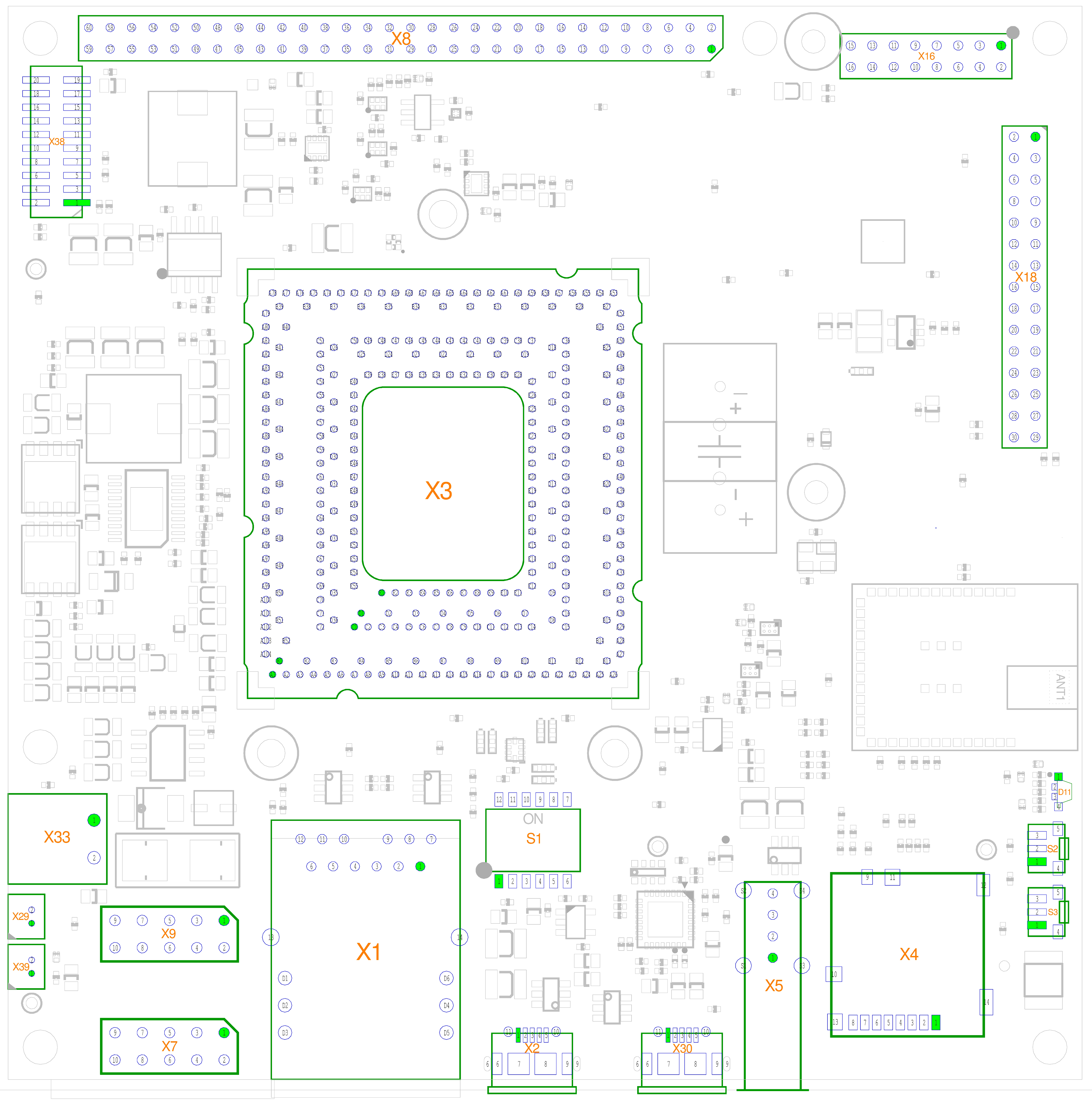
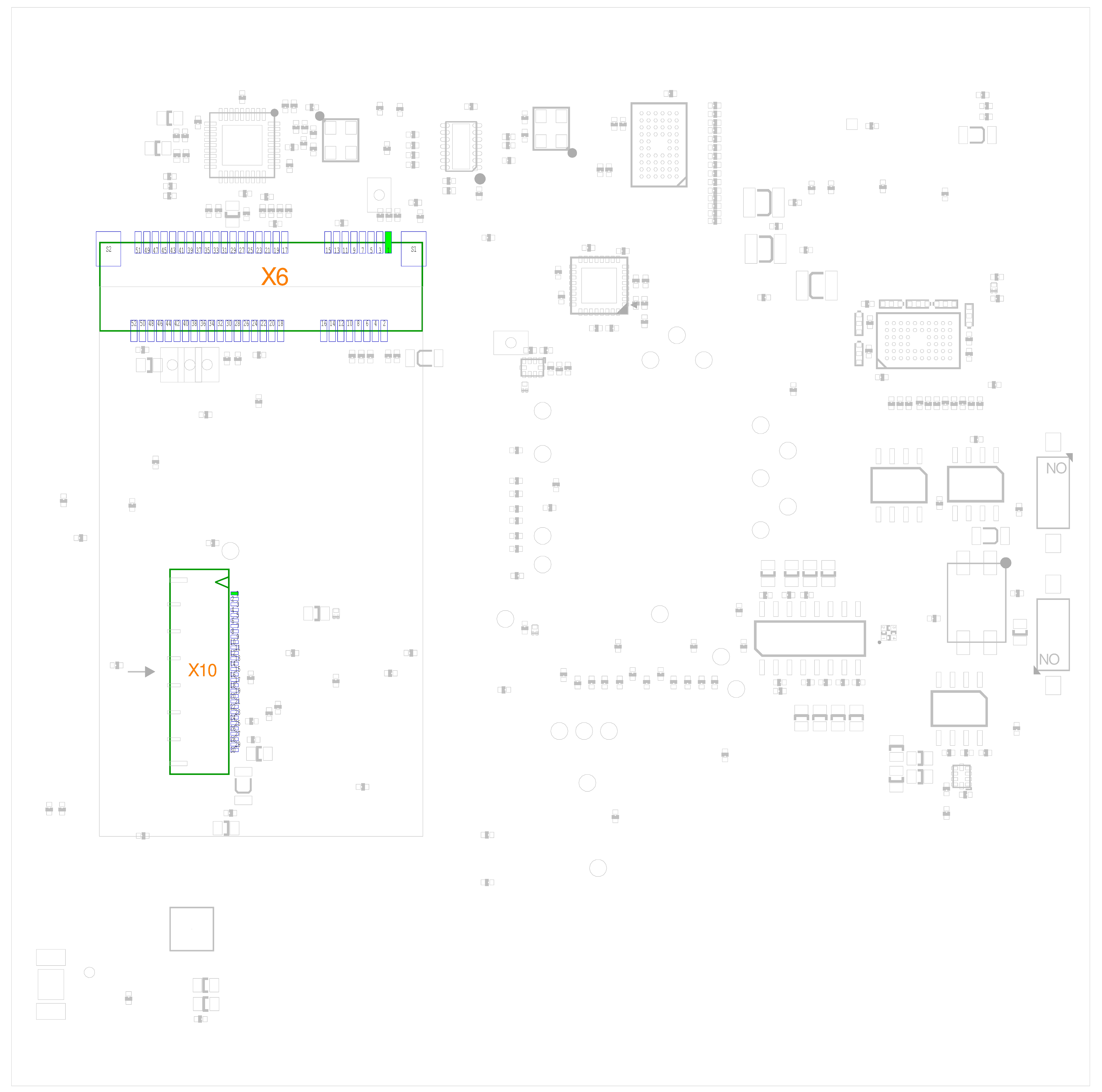
The phyBOARD‑Polis features many different interfaces and is equipped with the components listed in table L-862e.Ax phyCORE-i.MX 8M Mini/phyBOARD-Polis (1518.1a / 1532.1) HW Manual Head. For a more detailed description of each component, refer to the appropriate section listed in the table below. L-862e.Ax phyCORE-i.MX 8M Mini/phyBOARD-Polis (1518.1a / 1532.1) HW Manual Head and L-862e.Ax phyCORE-i.MX 8M Mini/phyBOARD-Polis (1518.1a / 1532.1) HW Manual Head highlight the location of each component for easy identification.
...
...
| secondary | phyBOARD-Polis Component Overview |
|---|---|
| tertiary | Connectors and Pin Headers |
| primary | phyCORE-i.MX 8M Mini on the phyBOARD-Polis |
...
Connectors and Pin Headers
| Anchor | ||||
|---|---|---|---|---|
|
This is a list of all available connectors on the phyBOARD-Polis.
...
| Warning | ||
|---|---|---|
| ||
Module connections must not exceed their expressed maximum voltage or current. Maximum signal input values are indicated in the corresponding controller manuals/datasheets. As damage from improper connections varies according to use and application, it is the user 's responsibility to must take appropriate safety measures to ensure that the module connections are protected from overloading through connected peripherals. |
...
LEDs
The phyBOARD-Polis is populated with one LED, which is user-programmable. L-862e.Ax phyCORE-i.MX 8M Mini/phyBOARD-Polis (1518.1a / 1532.1) HW Manual Head shows the location of the LED.
| Scroll Title | ||||||||||||||||||||||||||||
|---|---|---|---|---|---|---|---|---|---|---|---|---|---|---|---|---|---|---|---|---|---|---|---|---|---|---|---|---|
| ||||||||||||||||||||||||||||
|
...
...
...
Switches
...
...
| Anchor | ||||
|---|---|---|---|---|
|
The phyBOARD-Polis is populated with 3 switches. The tables below show their function:
...
- Boot Selection (see Multi-port Switch)
- SD-Card or WIFI Selection
- UART3 destination (A/V or FTDI) (see USB Debug)
...
...
Jumpers
...
| Anchor | ||||
|---|---|---|---|---|
|
The phyBOARD-Polis comes pre-configured with several solder jumpers (J). The jumpers enable the flexible configuration of a limited number of features for development purposes.
| Warning | ||
|---|---|---|
| ||
Due to the small footprint of the solder jumpers (J), PHYTEC does not recommend manual jumper modifications. This may also render the warranty invalid. Contact our sales team if you need jumper configurations different from the default configuration. |
...
. |
...
phyBOARD-Polis SBC Component Details
| Anchor | ||||
|---|---|---|---|---|
|
This section provides a more detailed look at the phyBOARD‑Polis components. Each subsection details a particular connector/interface for configuring that interface.
| Tip | ||
|---|---|---|
| ||
Where possible, we also provide any useful information regarding design consideration considerations for components. This can be used if you plan to design your own carrier board. |
...
. |
...
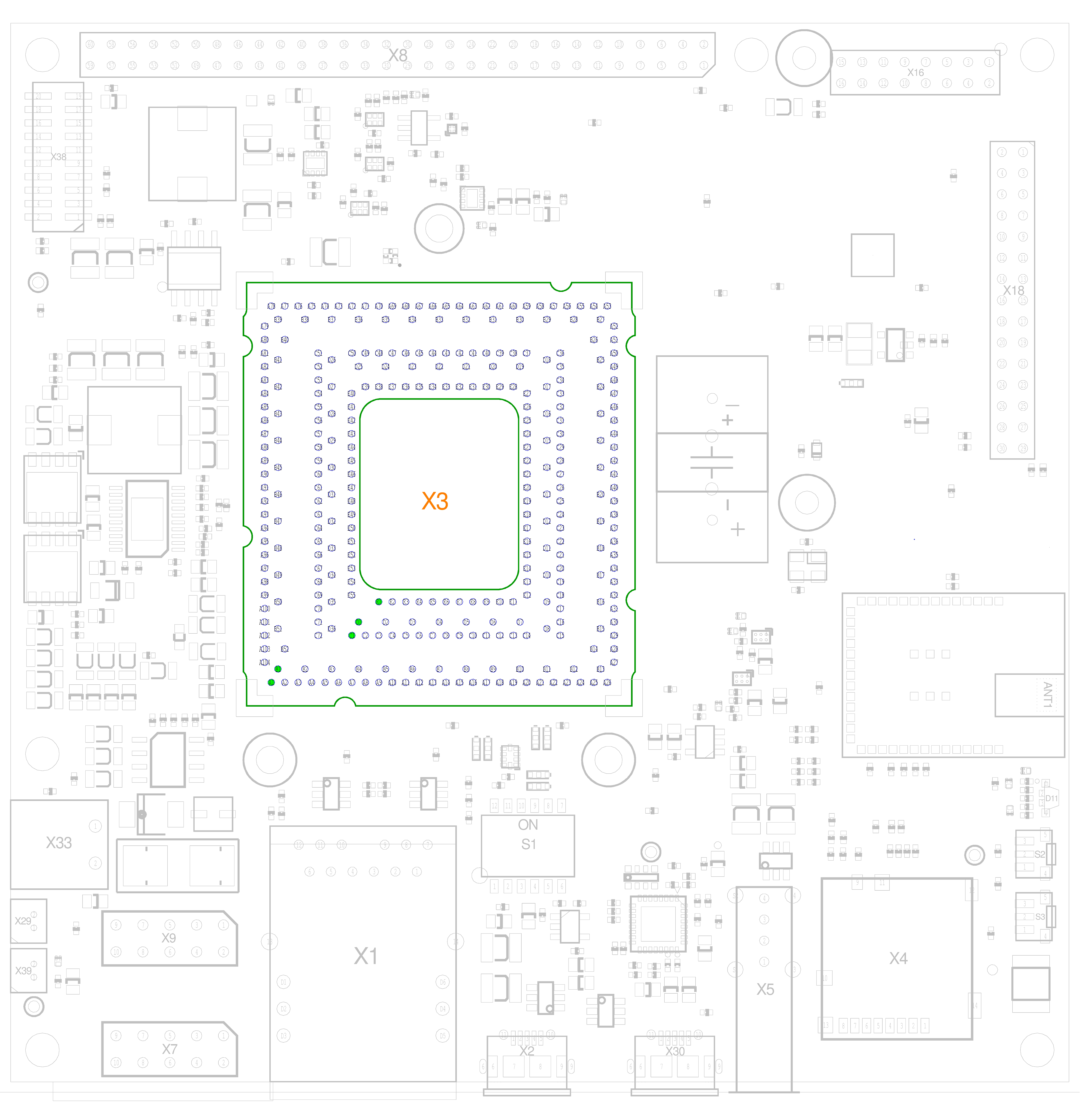
phyCORE-Connection (X3)
| Scroll Title | ||||
|---|---|---|---|---|
| ||||
...
...
Power
...
Supply (X33)
...
...
| Anchor | ||||
|---|---|---|---|---|
|
| Warning | ||
|---|---|---|
| ||
Do not change modules or jumper settings while the phyBOARD‑Polis is supplied with power! |
...
| Scroll Title | |||||||||||||||||||||||||||||
|---|---|---|---|---|---|---|---|---|---|---|---|---|---|---|---|---|---|---|---|---|---|---|---|---|---|---|---|---|---|
| |||||||||||||||||||||||||||||
|
...
Power Design Considerations
It is recommended to route high current rails, like the SOM supply voltage, as planes to keep series resistance at a minimum. The same thing should be applied to ground paths. For more information, see phyCORE-i.MX 8M Mini Power Consumption.
...
. For more information, see phyCORE-i.MX 8M Mini
...
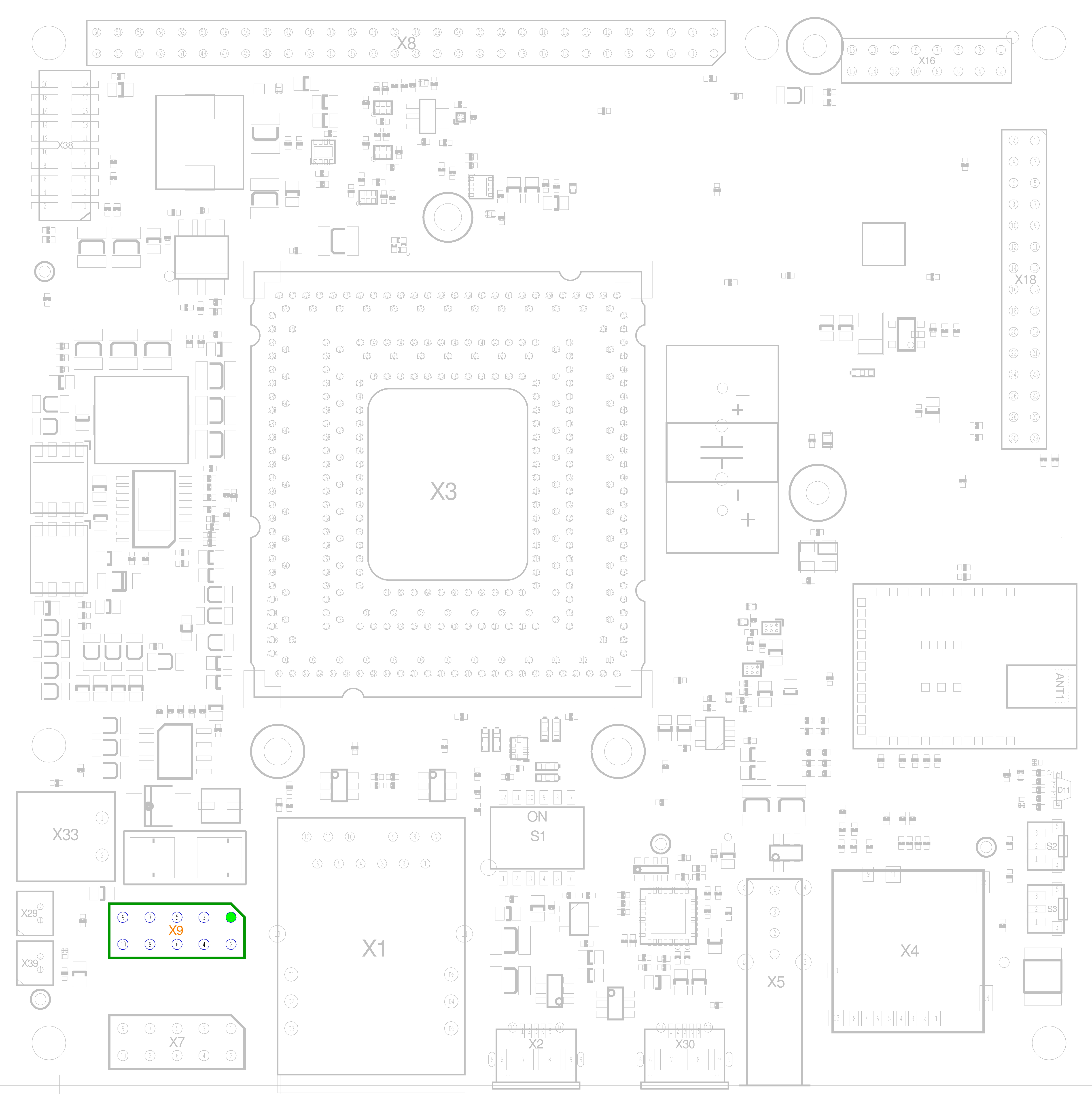
UART Connectivity (X8 and X9)
| Scroll Title | ||||
|---|---|---|---|---|
| ||||
...
| Scroll Title | ||||||||||||||||||||||||||||||||||||||||||||
|---|---|---|---|---|---|---|---|---|---|---|---|---|---|---|---|---|---|---|---|---|---|---|---|---|---|---|---|---|---|---|---|---|---|---|---|---|---|---|---|---|---|---|---|---|
| ||||||||||||||||||||||||||||||||||||||||||||
|
...
...
UART Design Consideration
...
When designing a custom carrier board, remember the TTL level is 3.3 V. Route signals as single-ended 50 Ohm lines.
...
...
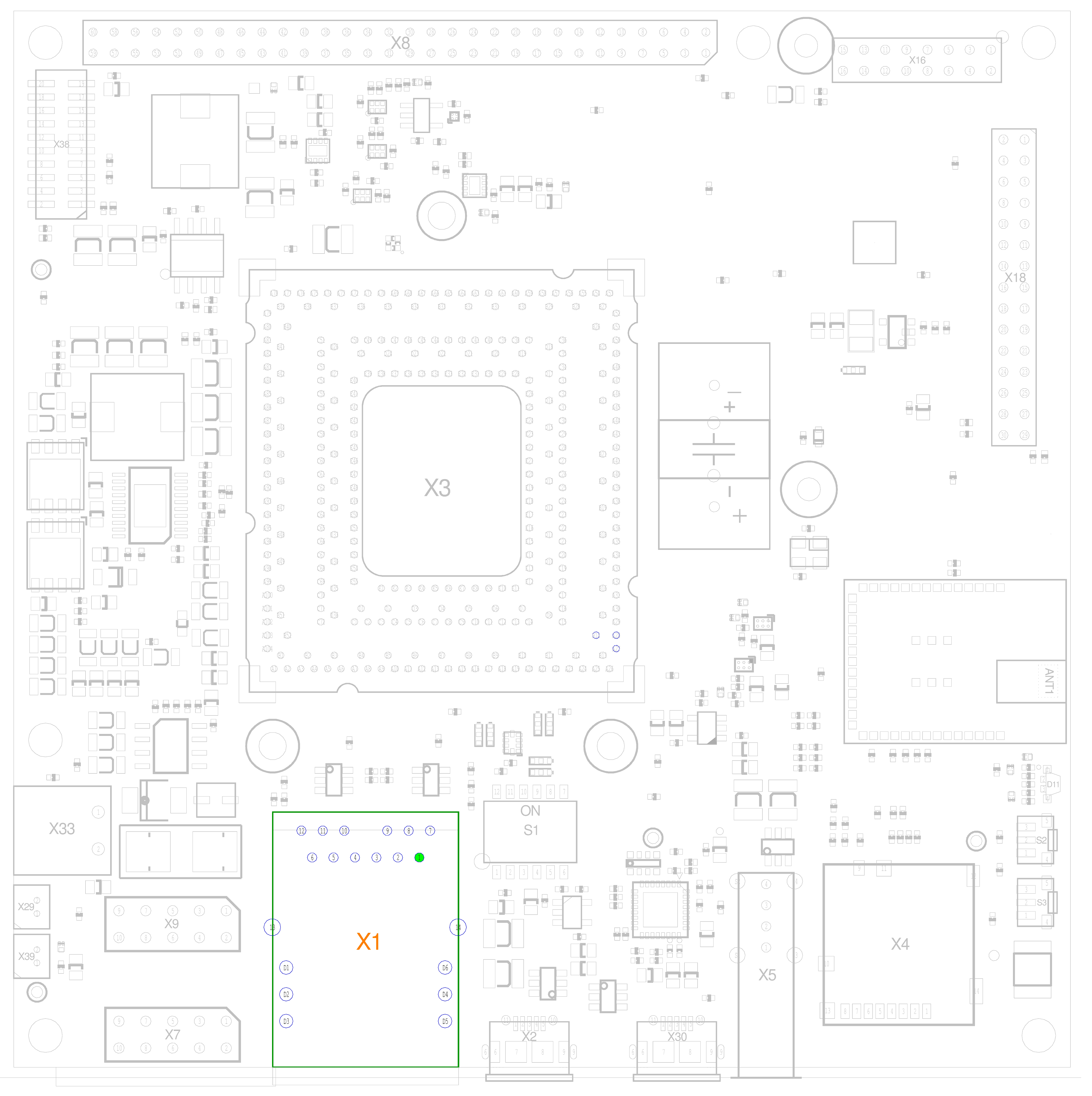
Ethernet Connectivity (X1)
...
| Scroll Title | ||||
|---|---|---|---|---|
| ||||
The phyBOARD‑Polis is equipped with an RJ45 connector supporting a 10/100/1000Base-T network connection. The LEDs for LINK LINK (green) and ACTIVITY (yellow) indication indications are integrated into the connector. The Ethernet transceiver supports Auto MDI-X, eliminating the need for a direct connect LAN or cross-over cable. They detect the TX and RX pins of the connected device and automatically configure the PHY TX and RX pins accordingly.
...
| Scroll Title | |||||||||||||||||||||||||||||||||||||||||||||||||||||||||||||||||||||||||||||||||||||||||||||||
|---|---|---|---|---|---|---|---|---|---|---|---|---|---|---|---|---|---|---|---|---|---|---|---|---|---|---|---|---|---|---|---|---|---|---|---|---|---|---|---|---|---|---|---|---|---|---|---|---|---|---|---|---|---|---|---|---|---|---|---|---|---|---|---|---|---|---|---|---|---|---|---|---|---|---|---|---|---|---|---|---|---|---|---|---|---|---|---|---|---|---|---|---|---|---|---|
| |||||||||||||||||||||||||||||||||||||||||||||||||||||||||||||||||||||||||||||||||||||||||||||||
|
...
Ethernet
...
Design Consideration
...
...
The data lanes should be routed with a differential impedance of 100 Ohm and kept as short as possible. The center taps of each pair's transformer have to be connected to GND through a 100nF capacitor. The LED pins are open-drain outputs of the SOM without a resistor, so they should be connected to the cathodes of the LEDs through a suitable resistor.
...
LED pins are open-drain outputs of the SOM without a resistor, so they should be connected to the cathodes of the LEDs through a suitable resistor.
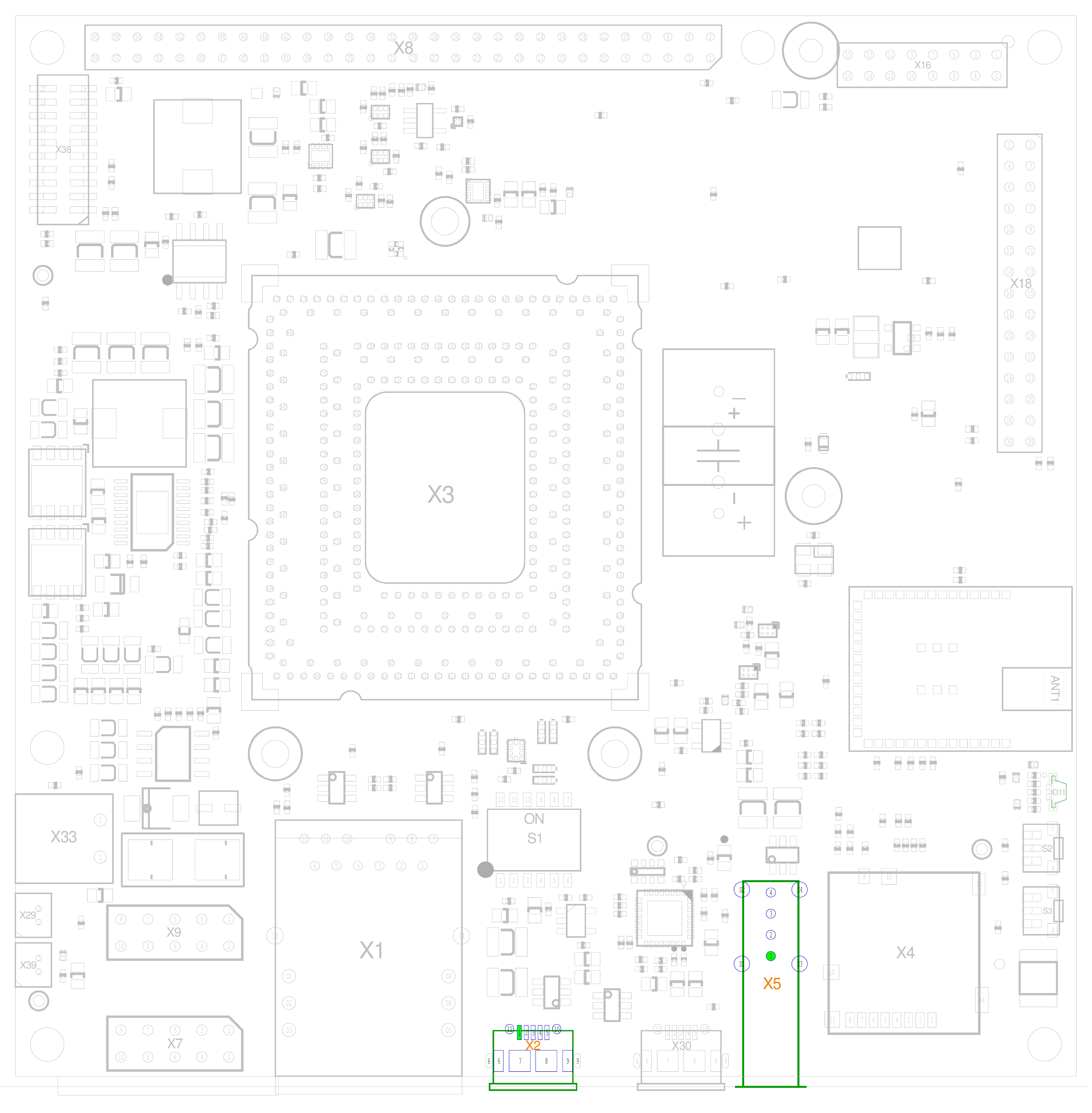
USB OTG and 2.0 Connectivity (X2 and X5)
| Scroll Title | ||||
|---|---|---|---|---|
| ||||
...
| Scroll Title | |||||||||||||||||||||||||||||||||||||||||||||||||||||||||||||||||
|---|---|---|---|---|---|---|---|---|---|---|---|---|---|---|---|---|---|---|---|---|---|---|---|---|---|---|---|---|---|---|---|---|---|---|---|---|---|---|---|---|---|---|---|---|---|---|---|---|---|---|---|---|---|---|---|---|---|---|---|---|---|---|---|---|---|
| |||||||||||||||||||||||||||||||||||||||||||||||||||||||||||||||||
|
...
...
...
USB Design Consideration
...
The data lanes should be routed with a differential impedance of 90 Ohm and kept as short as possible.
...
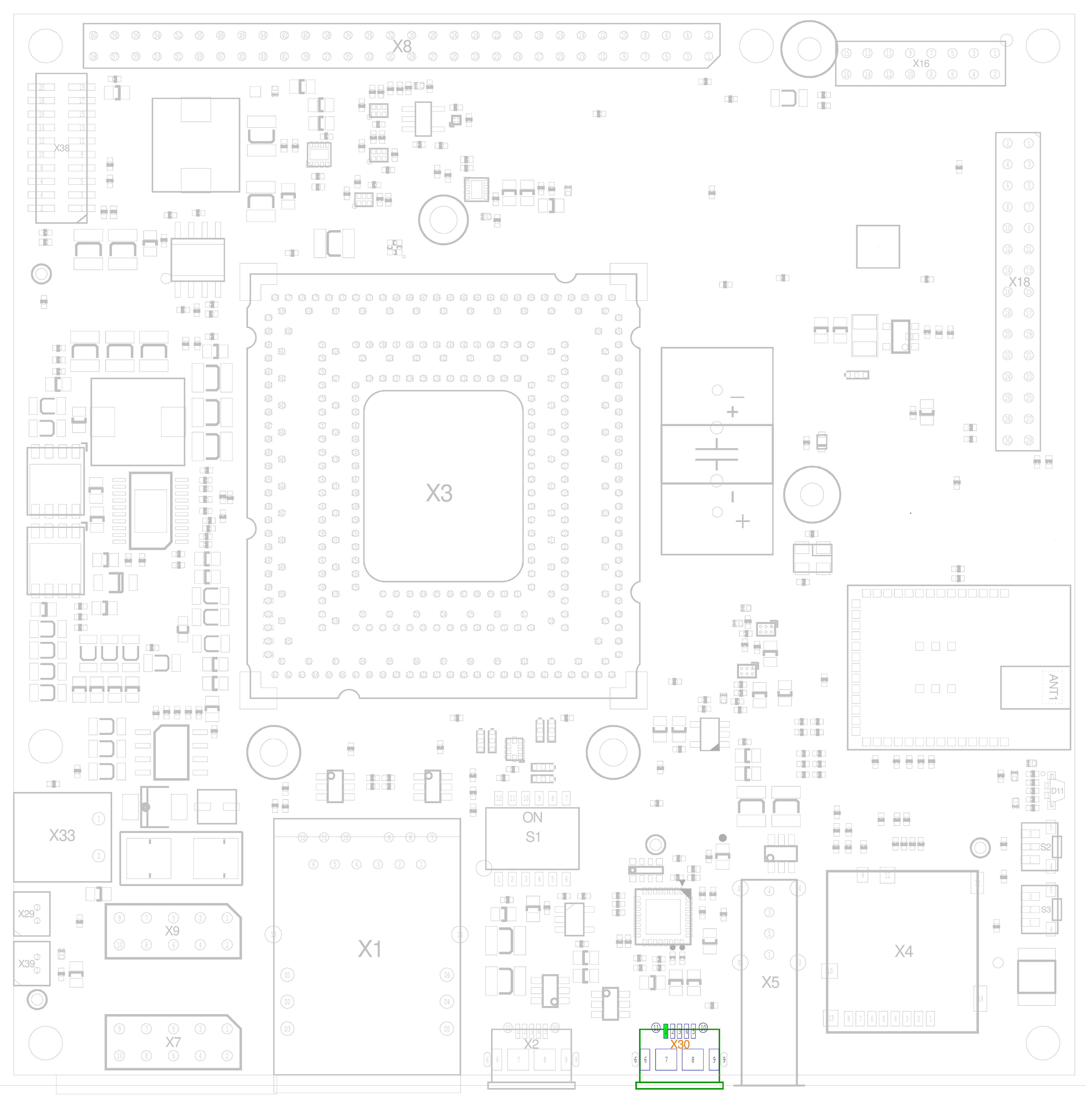
USB Debug (X30)
...
| Scroll Title | ||||
|---|---|---|---|---|
| ||||
...
| Scroll Title | ||||||||||||||||||||||||||||||||||||||||||||||||||||||||||||||||||||||||||||||||
|---|---|---|---|---|---|---|---|---|---|---|---|---|---|---|---|---|---|---|---|---|---|---|---|---|---|---|---|---|---|---|---|---|---|---|---|---|---|---|---|---|---|---|---|---|---|---|---|---|---|---|---|---|---|---|---|---|---|---|---|---|---|---|---|---|---|---|---|---|---|---|---|---|---|---|---|---|---|---|---|---|
| ||||||||||||||||||||||||||||||||||||||||||||||||||||||||||||||||||||||||||||||||
|
...
Debug Design Considerations
...
The UART data signals to the UART to USB converter should be routed as singled-ended signals with an impedance of 50 Ohm and kept as short as possible. The USB data lanes should be routed with a differential impedance of 90 Ohm and kept as short as possible.
...
possible.
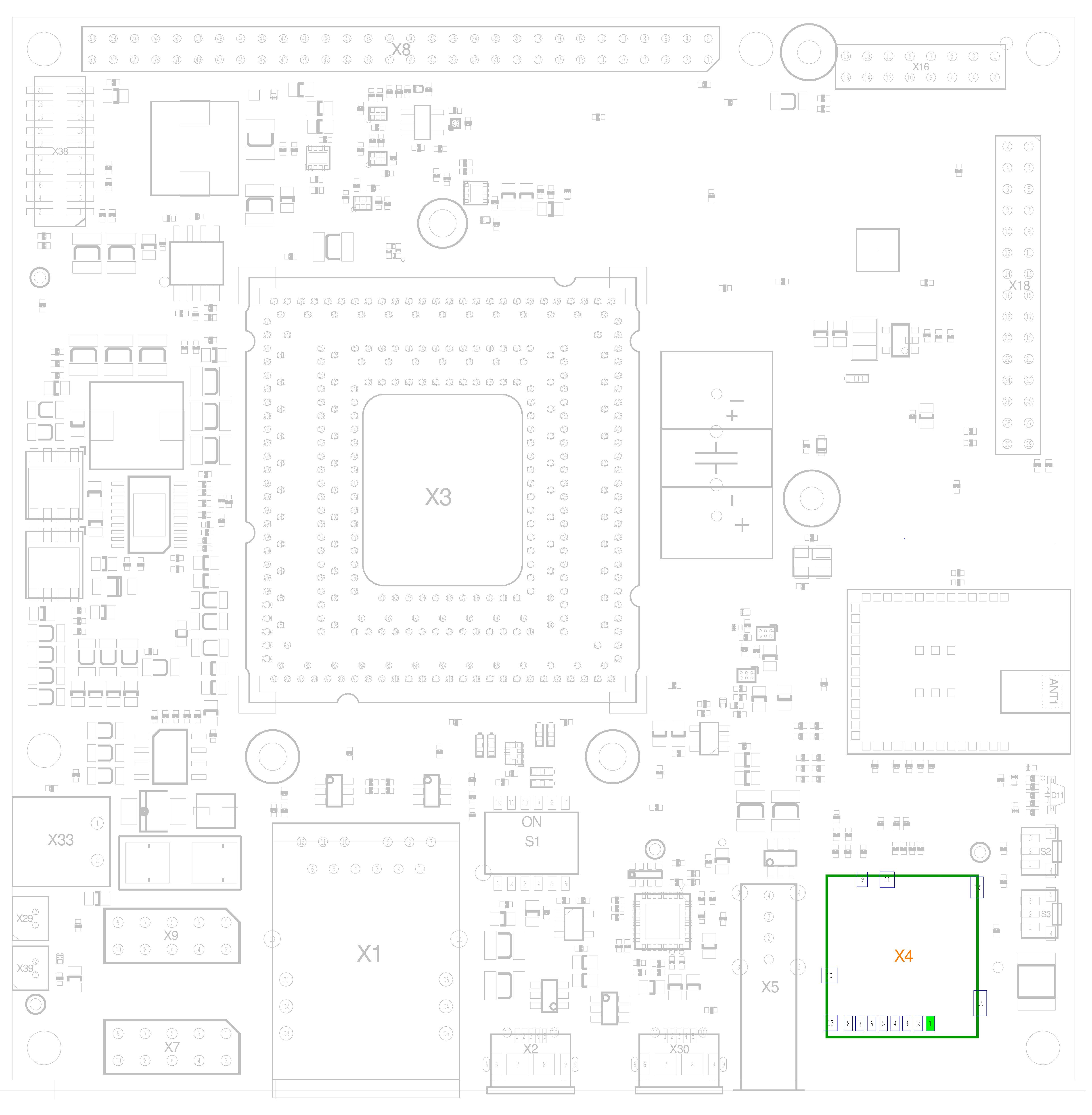
Secure Digital Memory / MultiMedia Card (X4)
| Scroll Title | ||||
|---|---|---|---|---|
| ||||
...
| Scroll Title | |||||||||||||||||||||||||||||||||||||||||||||||||||||||||||||||||||||||||||||||||||||||||||||||
|---|---|---|---|---|---|---|---|---|---|---|---|---|---|---|---|---|---|---|---|---|---|---|---|---|---|---|---|---|---|---|---|---|---|---|---|---|---|---|---|---|---|---|---|---|---|---|---|---|---|---|---|---|---|---|---|---|---|---|---|---|---|---|---|---|---|---|---|---|---|---|---|---|---|---|---|---|---|---|---|---|---|---|---|---|---|---|---|---|---|---|---|---|---|---|---|
| |||||||||||||||||||||||||||||||||||||||||||||||||||||||||||||||||||||||||||||||||||||||||||||||
|
...
SD / MM Card Design Considerations
Series resistors in data and clock signals should be placed as close as possible to the signal source. For I/O signals this means two resistors in one electric net are recommended. The voltage of the SD2 signal lanes is NVCC_SD2 and can switch between 1.8 V and 3.3 V. The supply voltage of the SD-Card remains 3.3 V and should not be connected to NCVV_SD2. All signals should be routed as 50 Ohm singledsingle-ended lines.
...
...
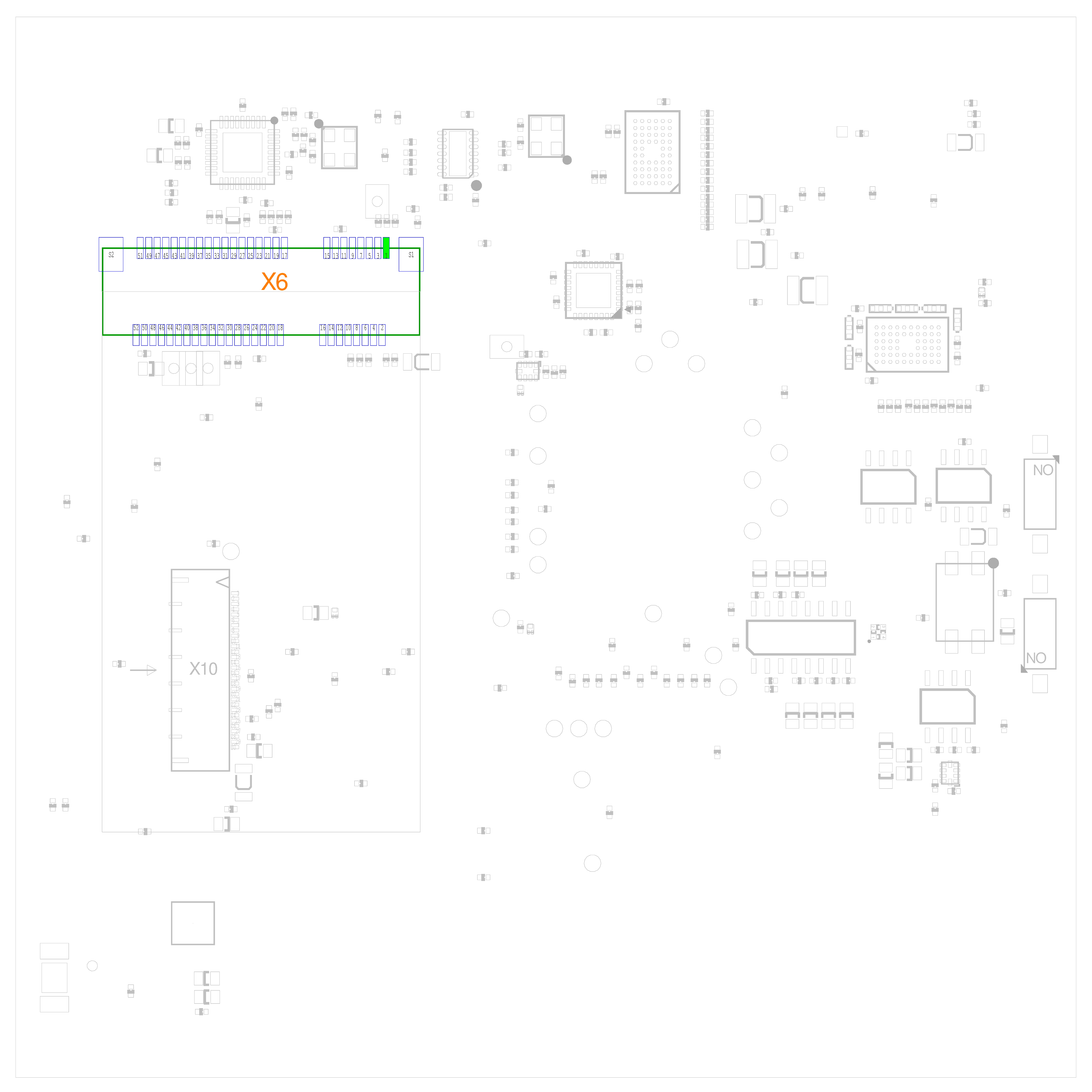
PCIe Connectivity (X6)
...
...
| Scroll Title | ||||
|---|---|---|---|---|
| ||||
...
| Scroll Title | |||||||||||||||||||||||||||||||||||||||||||||||||||||||||||||||||||||||||||||||||||||||||||||||||||||||||||||||||||||||||||||||||||||||||||||||||||||||||||||||||||||||||||||||||||||||||||||||||||||||||||||||||||||||||||||||||||||||||||||||||||||||||||||||||||||||||||||||||||||||||||||||||||||||
|---|---|---|---|---|---|---|---|---|---|---|---|---|---|---|---|---|---|---|---|---|---|---|---|---|---|---|---|---|---|---|---|---|---|---|---|---|---|---|---|---|---|---|---|---|---|---|---|---|---|---|---|---|---|---|---|---|---|---|---|---|---|---|---|---|---|---|---|---|---|---|---|---|---|---|---|---|---|---|---|---|---|---|---|---|---|---|---|---|---|---|---|---|---|---|---|---|---|---|---|---|---|---|---|---|---|---|---|---|---|---|---|---|---|---|---|---|---|---|---|---|---|---|---|---|---|---|---|---|---|---|---|---|---|---|---|---|---|---|---|---|---|---|---|---|---|---|---|---|---|---|---|---|---|---|---|---|---|---|---|---|---|---|---|---|---|---|---|---|---|---|---|---|---|---|---|---|---|---|---|---|---|---|---|---|---|---|---|---|---|---|---|---|---|---|---|---|---|---|---|---|---|---|---|---|---|---|---|---|---|---|---|---|---|---|---|---|---|---|---|---|---|---|---|---|---|---|---|---|---|---|---|---|---|---|---|---|---|---|---|---|---|---|---|---|---|---|---|---|---|---|---|---|---|---|---|---|---|---|---|---|---|---|---|---|---|---|---|---|---|---|---|---|---|---|---|---|---|---|---|---|---|---|---|---|---|---|---|---|---|---|---|---|---|---|---|
| |||||||||||||||||||||||||||||||||||||||||||||||||||||||||||||||||||||||||||||||||||||||||||||||||||||||||||||||||||||||||||||||||||||||||||||||||||||||||||||||||||||||||||||||||||||||||||||||||||||||||||||||||||||||||||||||||||||||||||||||||||||||||||||||||||||||||||||||||||||||||||||||||||||||
|
...
PCIe
...
Design Considerations
...
100nF AC-Coupling capacitors are placed close to output pins of the i.MX 8M Mini on the PCL-069 in series to the TX-Lanes. No further TX coupling capacitors are needed. The differential impedance should be 85 Ohm.
Camera Connections
...
100nF AC-Coupling capacitors are placed close to output pins of the
...
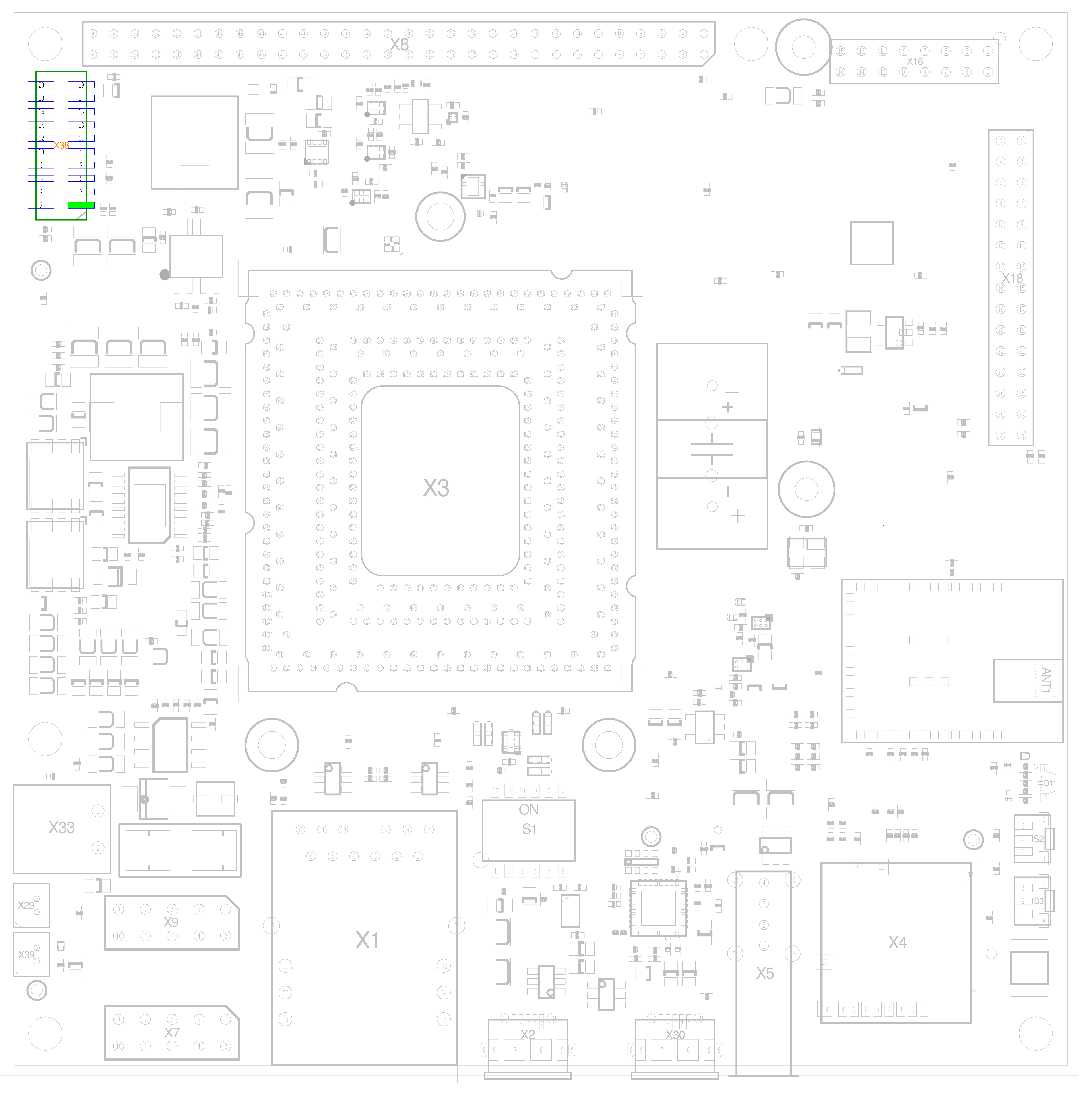
i.MX 8M Mini on the
...
PCL-069 in series to the TX-Lanes. No further TX coupling capacitors are needed. The differential impedance should be 85 Ohm.
Camera Connections
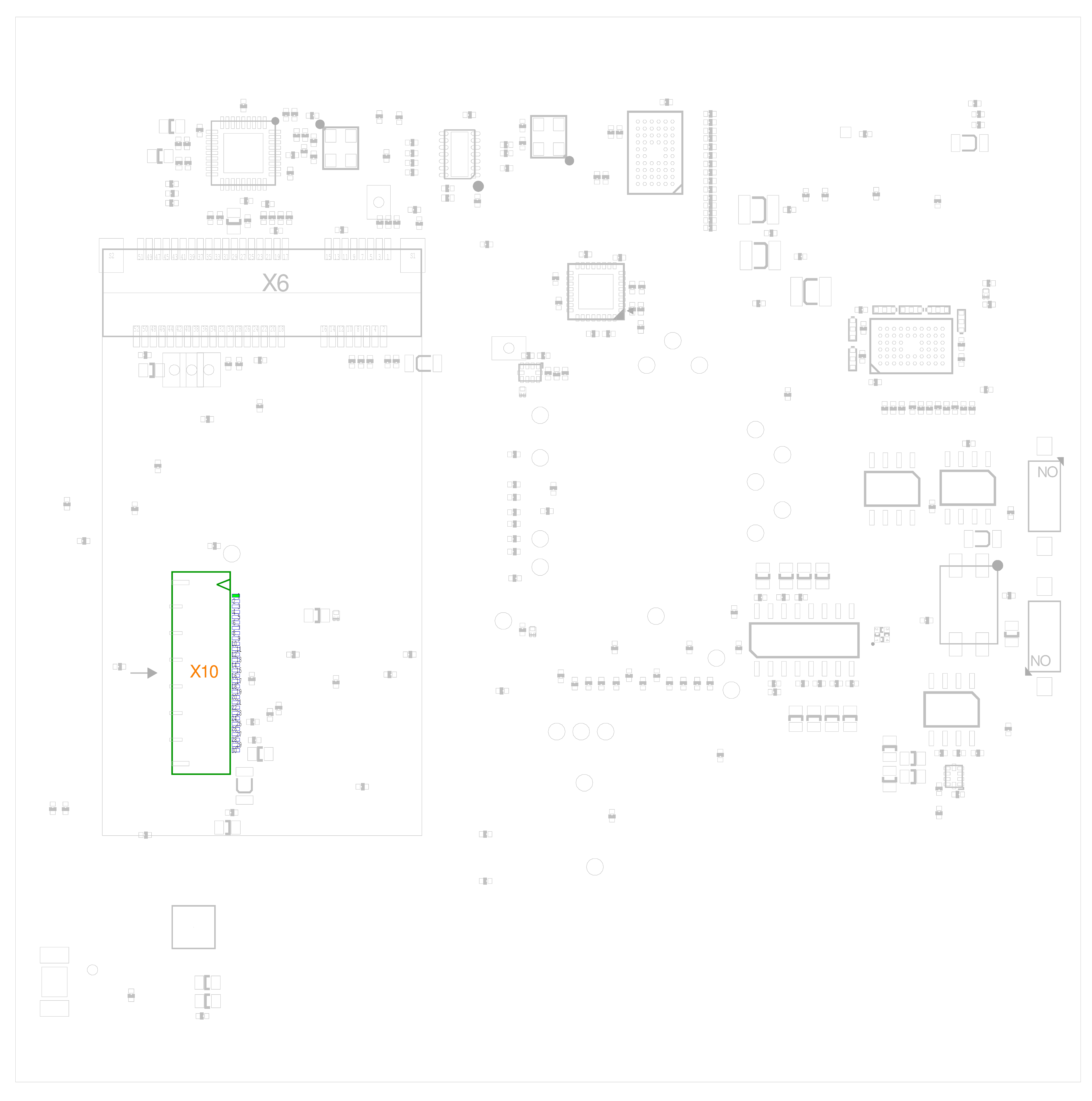
phyCAM-M MIPI CSI-2 Camera Connector (X10)
| Scroll Title | ||||
|---|---|---|---|---|
| ||||
...
| Scroll Title | |||||||||||||||||||||||||||||||||||||||||||||||||||||||||||||||||||||||||||||||||||||||||||||||||||||||||||||||||||||||||||||||||||||||||||||||||||||||||||||||||||||||||||||||
|---|---|---|---|---|---|---|---|---|---|---|---|---|---|---|---|---|---|---|---|---|---|---|---|---|---|---|---|---|---|---|---|---|---|---|---|---|---|---|---|---|---|---|---|---|---|---|---|---|---|---|---|---|---|---|---|---|---|---|---|---|---|---|---|---|---|---|---|---|---|---|---|---|---|---|---|---|---|---|---|---|---|---|---|---|---|---|---|---|---|---|---|---|---|---|---|---|---|---|---|---|---|---|---|---|---|---|---|---|---|---|---|---|---|---|---|---|---|---|---|---|---|---|---|---|---|---|---|---|---|---|---|---|---|---|---|---|---|---|---|---|---|---|---|---|---|---|---|---|---|---|---|---|---|---|---|---|---|---|---|---|---|---|---|---|---|---|---|---|---|---|---|---|---|---|---|
| |||||||||||||||||||||||||||||||||||||||||||||||||||||||||||||||||||||||||||||||||||||||||||||||||||||||||||||||||||||||||||||||||||||||||||||||||||||||||||||||||||||||||||||||
|
...
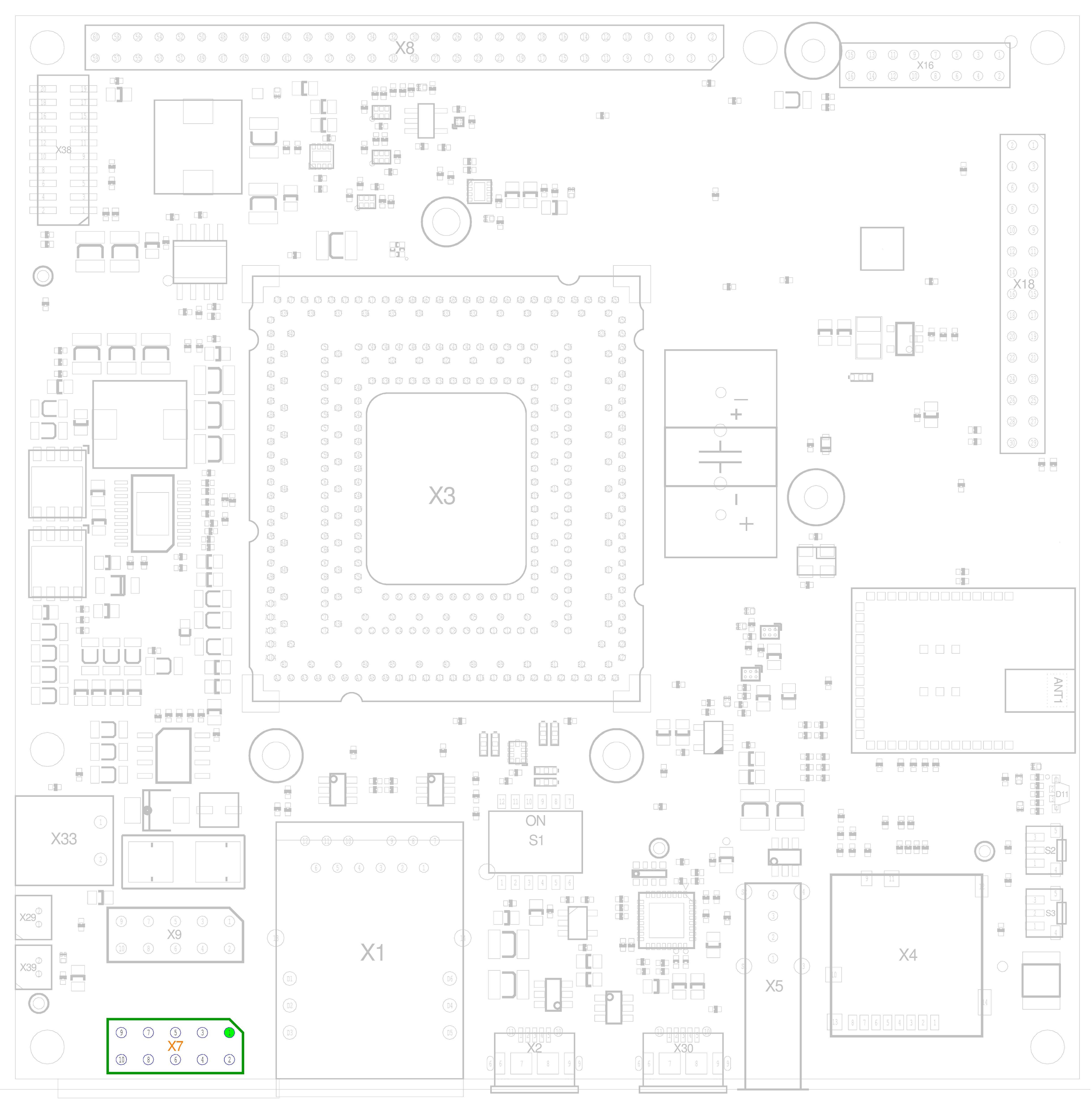
CAN FD (X7)
...
...
| Scroll Title | ||||
|---|---|---|---|---|
| ||||
...
| Scroll Title | ||||||||||||||||||||||||||||||||||||||||||||||||||||||||||||||||||||||||||
|---|---|---|---|---|---|---|---|---|---|---|---|---|---|---|---|---|---|---|---|---|---|---|---|---|---|---|---|---|---|---|---|---|---|---|---|---|---|---|---|---|---|---|---|---|---|---|---|---|---|---|---|---|---|---|---|---|---|---|---|---|---|---|---|---|---|---|---|---|---|---|---|---|---|---|
| ||||||||||||||||||||||||||||||||||||||||||||||||||||||||||||||||||||||||||
|
...
|
...
...
Audio/Video Connectors (X16 and X18)
...
| Scroll Title | ||||
|---|---|---|---|---|
| ||||
...
Cite summary showCitationLinks false local true
...
A/V Design Consideration
All signals should be routed as short as possible and as 50 Ohm single-ended lines.
...
as possible and as 50 Ohm single-ended lines.
Voice Array Connector (X38)
| Scroll Title | ||||
|---|---|---|---|---|
| ||||
...
| Scroll Title | |||||||||||||||||||||||||||||||||||||||||||||||||||||||||||||||||||||||||||||||||||||||||||||||||||||||||||||||||||
|---|---|---|---|---|---|---|---|---|---|---|---|---|---|---|---|---|---|---|---|---|---|---|---|---|---|---|---|---|---|---|---|---|---|---|---|---|---|---|---|---|---|---|---|---|---|---|---|---|---|---|---|---|---|---|---|---|---|---|---|---|---|---|---|---|---|---|---|---|---|---|---|---|---|---|---|---|---|---|---|---|---|---|---|---|---|---|---|---|---|---|---|---|---|---|---|---|---|---|---|---|---|---|---|---|---|---|---|---|---|---|---|---|---|---|---|
| |||||||||||||||||||||||||||||||||||||||||||||||||||||||||||||||||||||||||||||||||||||||||||||||||||||||||||||||||||
|
...
...
Voice Array
...
Design Considerations
All signals should be routed as short as possible and as 50 Ohm single-ended lines.
...
...
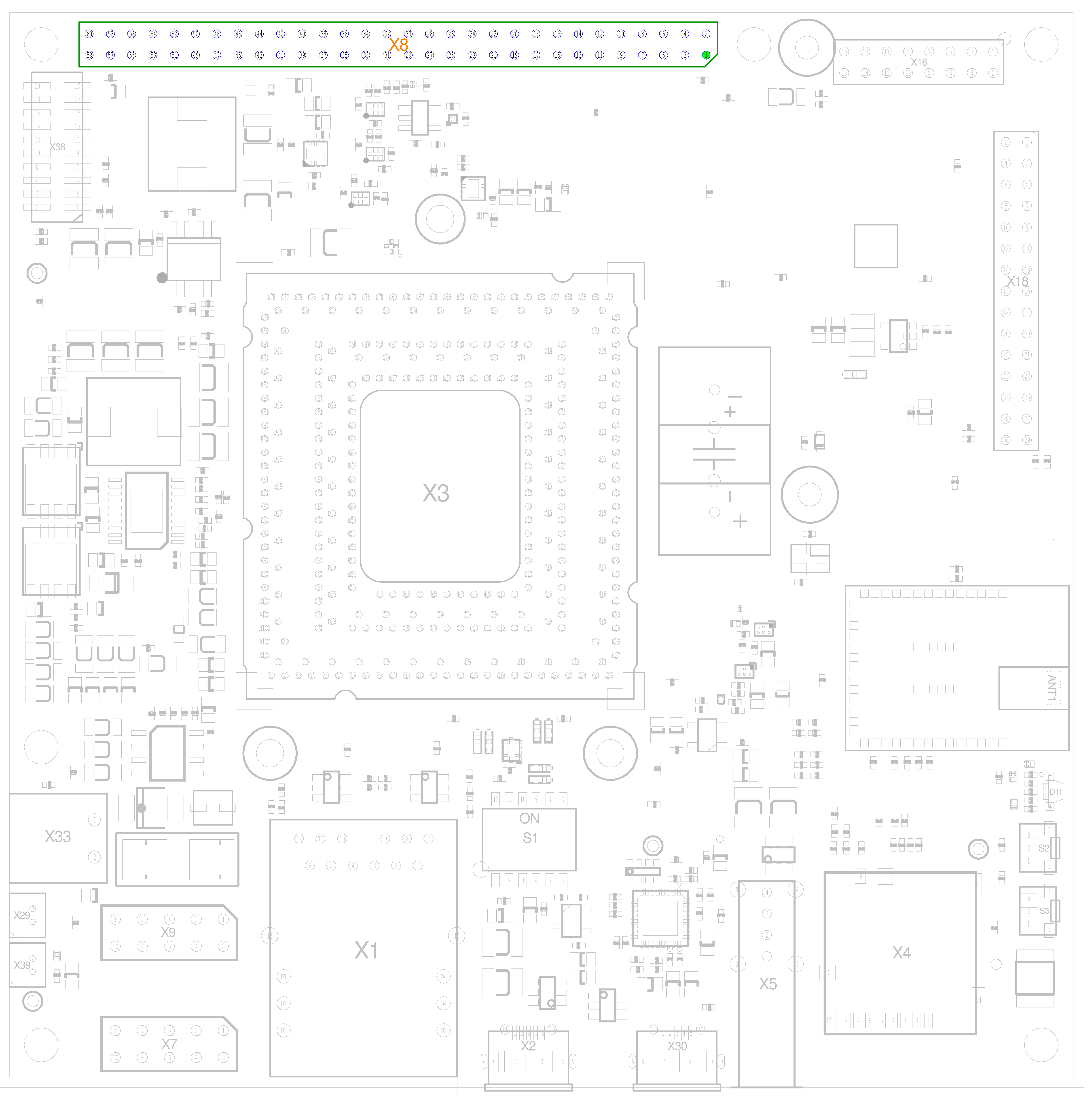
Expansion Connector (X8)
...
...
| Scroll Title | ||||
|---|---|---|---|---|
| ||||
...
| Scroll Title | |||||||||||||||||||||||||||||||||||||||||||||||||||||||||||||||||||||||||||||||||||||||||||||||||||||||||||||||||||||||||||||||||||||||||||||||||||||||||||||||||||||||||||||||||||||||||||||||||||||||||||||||||||||||||||||||||||||||||||||||||||||||||||||||||||||||||||||||||||||||||||||||||||||||||||||||||||||||||||||||||||||
|---|---|---|---|---|---|---|---|---|---|---|---|---|---|---|---|---|---|---|---|---|---|---|---|---|---|---|---|---|---|---|---|---|---|---|---|---|---|---|---|---|---|---|---|---|---|---|---|---|---|---|---|---|---|---|---|---|---|---|---|---|---|---|---|---|---|---|---|---|---|---|---|---|---|---|---|---|---|---|---|---|---|---|---|---|---|---|---|---|---|---|---|---|---|---|---|---|---|---|---|---|---|---|---|---|---|---|---|---|---|---|---|---|---|---|---|---|---|---|---|---|---|---|---|---|---|---|---|---|---|---|---|---|---|---|---|---|---|---|---|---|---|---|---|---|---|---|---|---|---|---|---|---|---|---|---|---|---|---|---|---|---|---|---|---|---|---|---|---|---|---|---|---|---|---|---|---|---|---|---|---|---|---|---|---|---|---|---|---|---|---|---|---|---|---|---|---|---|---|---|---|---|---|---|---|---|---|---|---|---|---|---|---|---|---|---|---|---|---|---|---|---|---|---|---|---|---|---|---|---|---|---|---|---|---|---|---|---|---|---|---|---|---|---|---|---|---|---|---|---|---|---|---|---|---|---|---|---|---|---|---|---|---|---|---|---|---|---|---|---|---|---|---|---|---|---|---|---|---|---|---|---|---|---|---|---|---|---|---|---|---|---|---|---|---|---|---|---|---|---|---|---|---|---|---|---|---|---|---|---|---|---|---|---|---|---|---|---|---|---|---|---|---|---|---|---|
| |||||||||||||||||||||||||||||||||||||||||||||||||||||||||||||||||||||||||||||||||||||||||||||||||||||||||||||||||||||||||||||||||||||||||||||||||||||||||||||||||||||||||||||||||||||||||||||||||||||||||||||||||||||||||||||||||||||||||||||||||||||||||||||||||||||||||||||||||||||||||||||||||||||||||||||||||||||||||||||||||||||
|
...
...
...
Expansion Connector Design Consideration
...
All signals should be routed as short as possible and as 50 Ohm single-ended lines.
...
.
...
I2C Connectivity
The I2C interfaces of the i.MX 8M Mini are available at different connectors on the phyBOARD‑Polis. The following table provides a list of the connectors and pins with I2C connectivity:
| Scroll Title | |||||||||||||||||||||||||||||||||||||||||||||||||||||||||||||||||
|---|---|---|---|---|---|---|---|---|---|---|---|---|---|---|---|---|---|---|---|---|---|---|---|---|---|---|---|---|---|---|---|---|---|---|---|---|---|---|---|---|---|---|---|---|---|---|---|---|---|---|---|---|---|---|---|---|---|---|---|---|---|---|---|---|---|
| |||||||||||||||||||||||||||||||||||||||||||||||||||||||||||||||||
|
Onboard Functionalities
...
|
Onboard Functionalities
...
Trusted Platform Module (TPM)
The phyBOARD-Polis is equipped with a Trusted Platform Module (TPM). The TPM is a chip developed, produced, tested, and certified according to the TCG specification that enhances the board with additional security functions. These security functions include the generation and secure storage (in the hardware) of keys for the authentication and identification of communication participants (SSH, server, cloud, etc.) and data, which can also be encrypted.
...
| Tip | ||
|---|---|---|
| ||
For more information about your security needs, contact a PHYTEC salesperson. |
...
...
Wireless WLAN and Bluetooth Transceiver Module
...
...
| Anchor | ||||
|---|---|---|---|---|
|
The phyBOARD-Polis is equipped with a Wireless WLAN and Bluetooth Transceiver Module that is capable of providing WLAN and Bluetooth functionality. The module requires a UART with handshake capability and a 4-bit SDIO interface. The module is connected to the SOM through the following interfaces:
| Scroll Title | |||||||||||||||||||||||||||||||||||||||||||||||||||||||||||||||||||||||||||||||||||||||||||||||
|---|---|---|---|---|---|---|---|---|---|---|---|---|---|---|---|---|---|---|---|---|---|---|---|---|---|---|---|---|---|---|---|---|---|---|---|---|---|---|---|---|---|---|---|---|---|---|---|---|---|---|---|---|---|---|---|---|---|---|---|---|---|---|---|---|---|---|---|---|---|---|---|---|---|---|---|---|---|---|---|---|---|---|---|---|---|---|---|---|---|---|---|---|---|---|---|
| |||||||||||||||||||||||||||||||||||||||||||||||||||||||||||||||||||||||||||||||||||||||||||||||
|
...
...
LEDs and Switches
...
| Scroll Title | ||||
|---|---|---|---|---|
| ||||
...
...
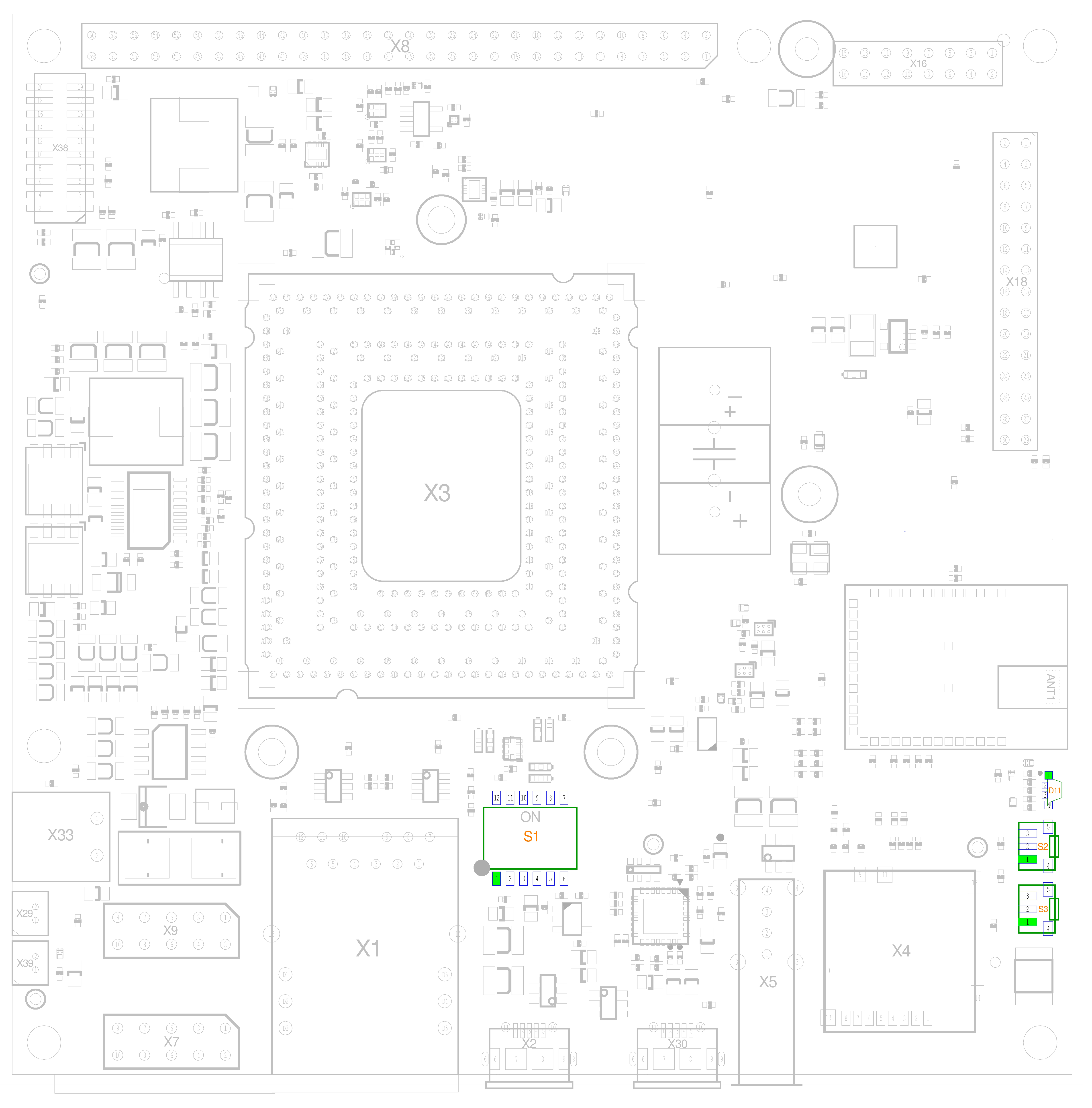
Multicolor (RGB) LED (D11)
...
...
The phyBOARD-Polis provides one multicolor (RGB) LED (D11). The table below shows the signals that control colors:
...
All signals should be routed as short as possible and as 50 Ohm single-ended lines.
...
.
...
Switches
Multi-port Switch (S1)
The phyBOARD‑Polis features a multi-port switch with six individually switchable ports. This switch controls the SOM boot mode, SOM boot configuration, UART functionality, and USB configuration when i.MX 8M NANO is mounted on the carrier board. The figures below show a visual representation of each S1 switch setting:
...
The phyBOARD-Polis is equipped with an ON/OFF button at S3. For more information on the ON/OFF switch, refer to the i.XM 8M Mini Reference Manual.
...
Revision History
| Scroll Title | |||||||||||||||||||||||||||||||||||
|---|---|---|---|---|---|---|---|---|---|---|---|---|---|---|---|---|---|---|---|---|---|---|---|---|---|---|---|---|---|---|---|---|---|---|---|
| |||||||||||||||||||||||||||||||||||
|
...

